Biolar transistor

a transistor and biolar technology, applied in the field of biolar transistors, can solve problems such as practicability difficulties in manufacturing

Inactive Publication Date: 2004-05-20
NEC CORP
View PDF2 Cites 17 Cited by
  • Summary
  • Abstract
  • Description
  • Claims
  • Application Information

AI Technical Summary

Benefits of technology

[0018] In the present invention, a non-doped SiGe layer prevents thermal diffusion of impurities in a base layer into an emitter layer side.
[0028] The base-emitter junction capacitance C.sub.BE takes on a small value because the composition ratio of Ge in the emitter layer side of the SiGe base layer is decreased with increasing proximity to the emitter layer side, and the non-doped layers (the non-doped SiGe layer and the non-doped Si layer) are provided between the emitter layer and the base layer. The direct-current gain .beta. takes on a large value because the composition ratio of Ge is adjusted at a predetermined value or more in the emitter layer-side end of the SiGe base layer. In this manner, with respect to the bipolar transistor according to the present invention, the minimum noise FIG. 48 reduced than ever.
[0048] In FIG. 7, the composition ratio of Ge in the SiGe base region 77 gradually decreases partially in the emitter region side with increasing proximity to the emitter region side. Furthermore, the composition ratio of Ge in the non-doped SiGe region 76 is smaller than the composition ratio of Ge in the emitter region-side end of the SiGe base region 77. By these changes in the composition ratio of Ge and the above-described restriction on the thermal diffusion of boron, a small base-emitter junction capacitance C.sub.BE can be achieved. Since the composition ratio of Ge is adjusted at a relatively high value (6%) in the emitter region-side end of the SiGe base region 77, a high direct-current gain .beta. can be achieved. In this manner, a small minimum noise figure can be realized with respect to the bipolar transistor having the profile shown in FIG. 7.

Problems solved by technology

However, a problem occurs in that manufacture is practically difficult with respect to a device having the profile shown in FIG. 4.

Method used


Image

  • Biolar transistor
  • Biolar transistor
  • Biolar transistor

Examples


example 2

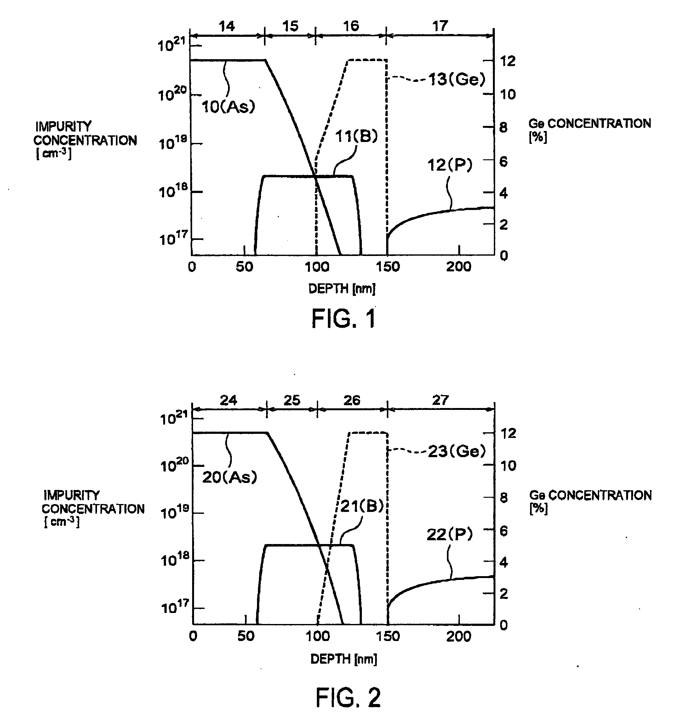
[0058] A bipolar transistor according to a second example of the present invention will be described with reference to FIG. 11. FIG. 11 shows the distributions of the impurity concentration and the composition ratio of Ge in the depth direction of the bipolar transistor according to the second example. In FIG. 11, a first solid line 110 indicates a concentration of arsenic, while arsenic is a dopant in an n-type emitter. A second solid line 111 indicates a concentration of boron, while boron is a dopant in a p-type base. A third solid line 112 indicates a concentration of phosphorus, while phosphorus in a dopant in an n-type collector. A broken line 113 indicates a composition ratio of Ge. A first double-headed arrow 114 indicates an emitter poly-Si region. A second double-headed arrow 115 indicates a single crystal Si region (non-doped Si region). The single crystal Si region is non-doped in an As-depo state, and finally a part thereof becomes of the n-type because of diffusion of ...

example 3

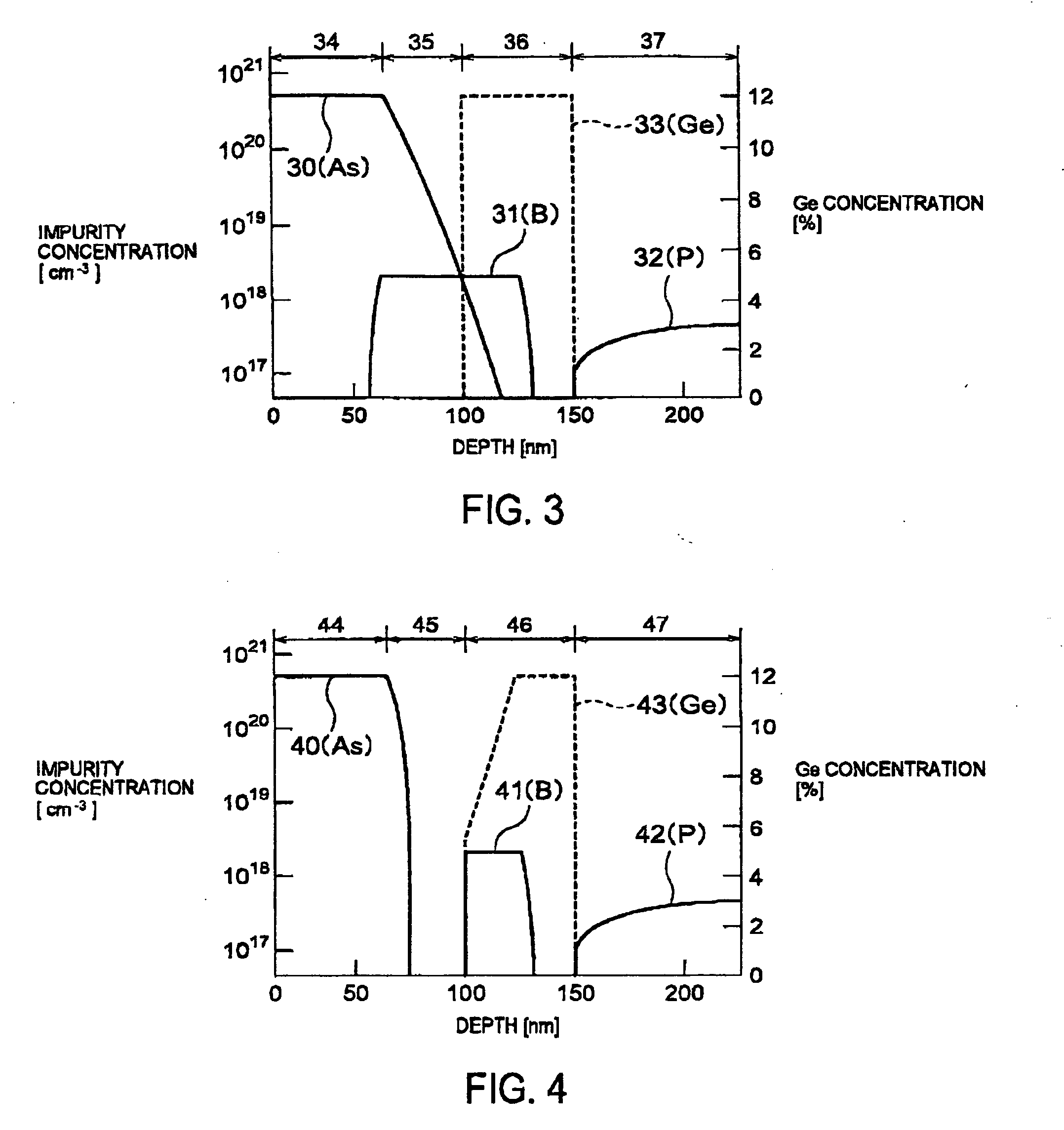
[0060] A bipolar transistor according to a third example of the present invention will be described with reference to FIG. 12. FIG. 12 shows the distributions of the impurity concentration and the composition ratio of Ge in the depth direction of the bipolar transistor according to the third example. In FIG. 12, a first solid line 120 indicates a concentration of arsenic, while arsenic is a dopant in an n-type emitter. A second solid line 121 indicates a concentration of boron, while boron is a dopant in a p-type base. A third solid line 122 indicates a concentration of phosphorus, while phosphorus is a dopant in an n-type collector. A broken line 123 indicates a composition ratio of Ge. A first double-headed arrow 124 indicates an emitter poly-Si region. A second double-headed arrow 125 indicates a single crystal Si region (a region assumed to be a non-doped Si region). The single crystal Si region is of the p-type having a low impurity concentration in an As-depo state, and finall...

example 4

[0064] A bipolar transistor according to a fourth example of the present invention will be described with reference to FIG. 13. FIG. 13 shows the distributions of the impurity concentration and the composition ratio of Ge in the depth direction of the bipolar transistor according to the fourth example. In FIG. 13, a first solid line 130 indicates a concentration of arsenic, while arsenic is a dopant in an n-type emitter. A second solid line 131 indicates a concentration of boron, while boron is a dopant in a p-type base. A third solid line 132 indicates a concentration of phosphorus, while phosphorus in a dopant in an n-type collector. A broken line 133 indicates a composition ratio of Ge. A first double-headed arrow 134 indicates an emitter poly-Si region. A second double-headed arrow 135 indicates a single crystal Si region (a region assumed to be a non-doped Si region). The single crystal Si region is non-doped in an As-depo state, and finally becomes of the n-type because of dif...


PUM


Abstract

In a bipolar transistor including a base layer made of SiGe, a non-did SiGe layer and a non-doped Si layer are provided between the base layer and an emitter layer. The composition ratio of Ge in the emitter side of SiGe base layer is decreased with increasing proximity to the emitter side, and the composition ratio of Ge in the non-doped SiGe layer is a smaller than the composition ratio of Ge at the emitter layer-side end of the SiGe base layer. In this manner, restriction is put on the diffusion of boron from the base layer to the emitter side, and the base-emitter junction capacitance CBE reduced. Furthermore, the direct-current gain beta can be improved by increasing the composition of Ge at the emitter end of the SiGe base layer to more than or equal to a predetermined value.

Description

[0001] The present invention relates to a semiconductor device. In particular, the present invention relates to a bipolar transistor including a base layer made of silicon germanium (SiGe).[0002] A minimum noise figure of a bipolar transistor is effectively reduced by reduction in the base-emitter junction capacitance C.sub.BE, an improvement in the direct-current gain .beta., and / or reduction in the sum, R.sub.B+R.sub.E, of a base resistance R.sub.B and an emitter resistance R.sub.E.[0003] With respect to a SiGe-base bipolar transistor using SiGe as a base material, since the band gap of SiGe is narrower than the band gap of silicon (Si) or polysilicon (Poly-Si) serving as a material for an emitter, sufficiently large direct-current gain .beta. can be achieved by increasing the impurity concentration of the base, and therefore, by reducing the base resistance R.sub.E. With respect to the SiGe-base bipolar transistor, the composition ratio of Ge in the base is increased in a directi...

Claims


Application Information

Patent Timeline
Patent Type & Authority Applications(United States)
IPC IPC(8): H01L21/331H01L29/10H01L29/36H01L29/737
CPCH01L29/1004H01L29/7378H01L29/36
Inventor MATSUNO, NORIAKI
Owner NEC CORP
Why Eureka
Try Eureka