Preventing Contamination in Integrated Circuit Manufacturing Lines

a manufacturing line and integrated circuit technology, applied in the field of integrated circuit manufacturing lines, can solve the problems of increasing the negative effects of amcs on ic manufacturing, affecting device performance or metrology accuracy, and so as to improve yield and performance. the effect of reducing the exposure of wafers

Active Publication Date: 2008-12-11
TAIWAN SEMICON MFG CO LTD
View PDF30 Cites 19 Cited by
  • Summary
  • Abstract
  • Description
  • Claims
  • Application Information

AI Technical Summary

Benefits of technology

[0012]The advantageous features of the present invention include reduced exposure of wafers to detrimental

Problems solved by technology

When exposed to the open environment, wafers are vulnerable to the attacks of adverse substances such as moisture, oxygen, and various airborne molecular contaminants (AMC) sources, which include etching byproduct solvents, perfumes, storage materials, chamber residual gases, etc.
As the semiconductor processes precede into the nanometer domain, the negative effects of AMCs on IC manufacturing become increasingly more severe.
In some critical stages, AMCs have posted serious problems impacting either device performance or metrology accuracy.
For example, in the formation of copper features in metallization layers, due to the very small size of copper features, the reaction caused by oxygen, moisture, and the AMC sources causes the increase in RC delay, and even the reduction in productio

Method used


Image

  • Preventing Contamination in Integrated Circuit Manufacturing Lines
  • Preventing Contamination in Integrated Circuit Manufacturing Lines
  • Preventing Contamination in Integrated Circuit Manufacturing Lines

Examples


Embodiment Construction

[0018]The making and using of the presently preferred embodiments are discussed in detail below. It should be appreciated, however, that the present invention provides many applicable inventive concepts that can be embodied in a wide variety of specific contexts. The specific embodiments discussed are merely illustrative of specific ways to make and use the invention, and do not limit the scope of the invention.

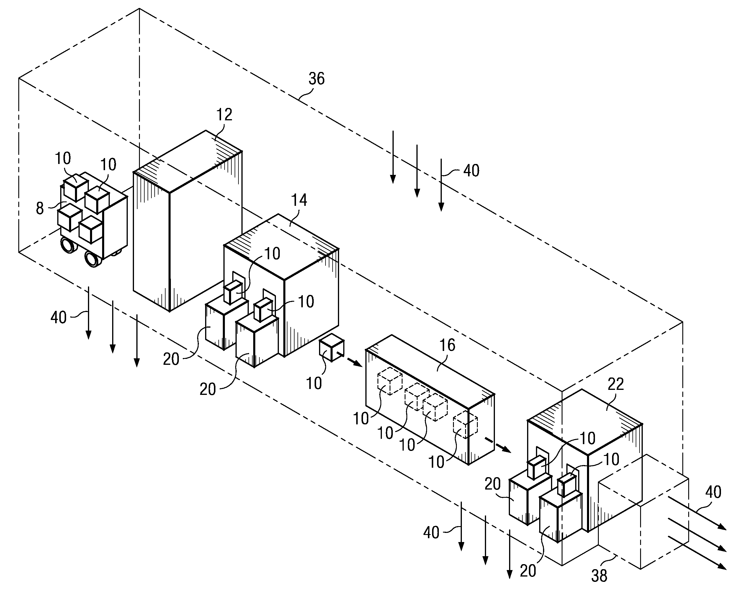
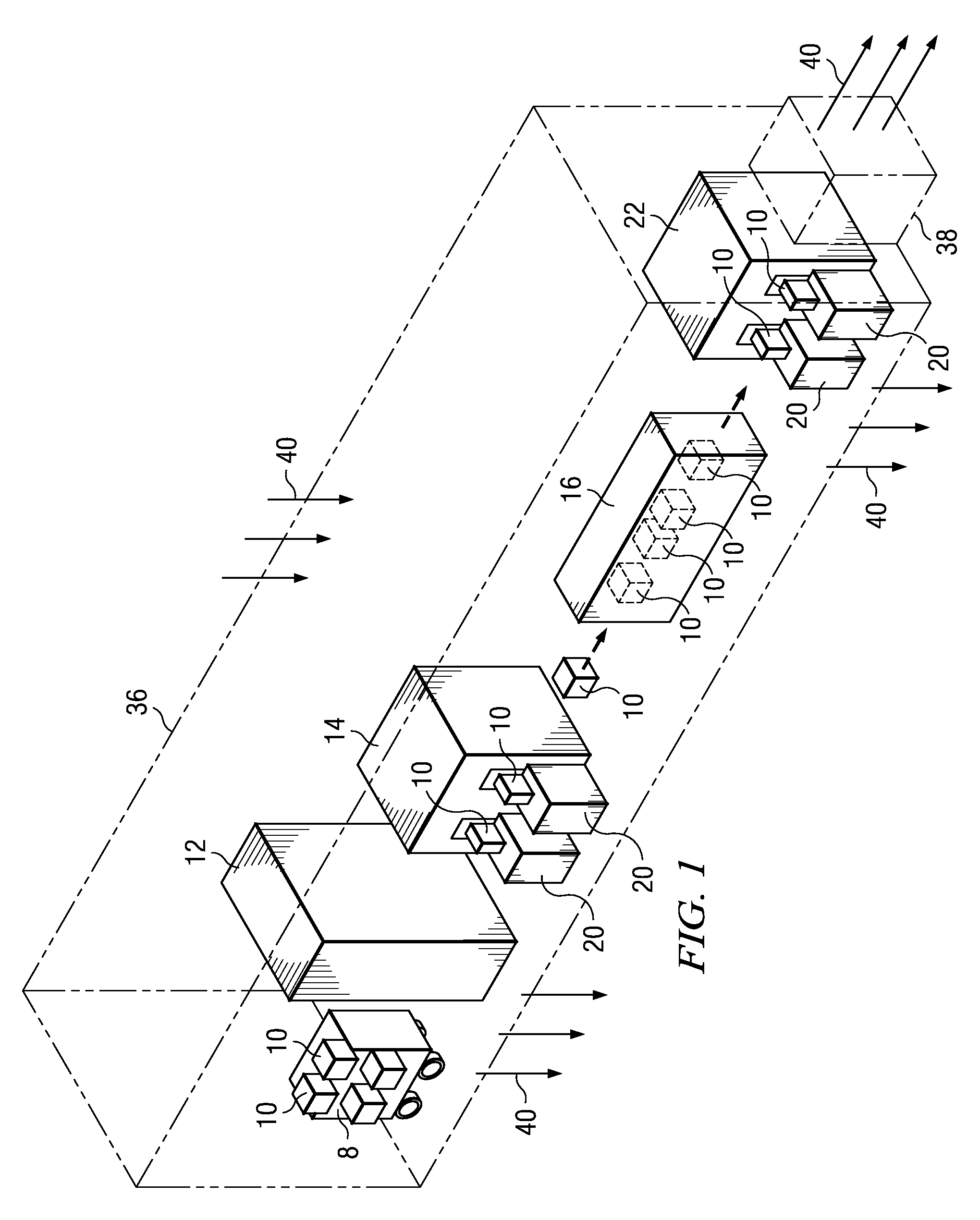
[0019]FIG. 1 illustrates an exemplary manufacturing line, which includes trolley 8, stocker 12, production tools 14 and 22, and wafer transport channel 16. Trolley 8 and wafer transport channel 16 are used to transport wafer holders 10, which may be cassettes or front opening unified pods (FOUP).

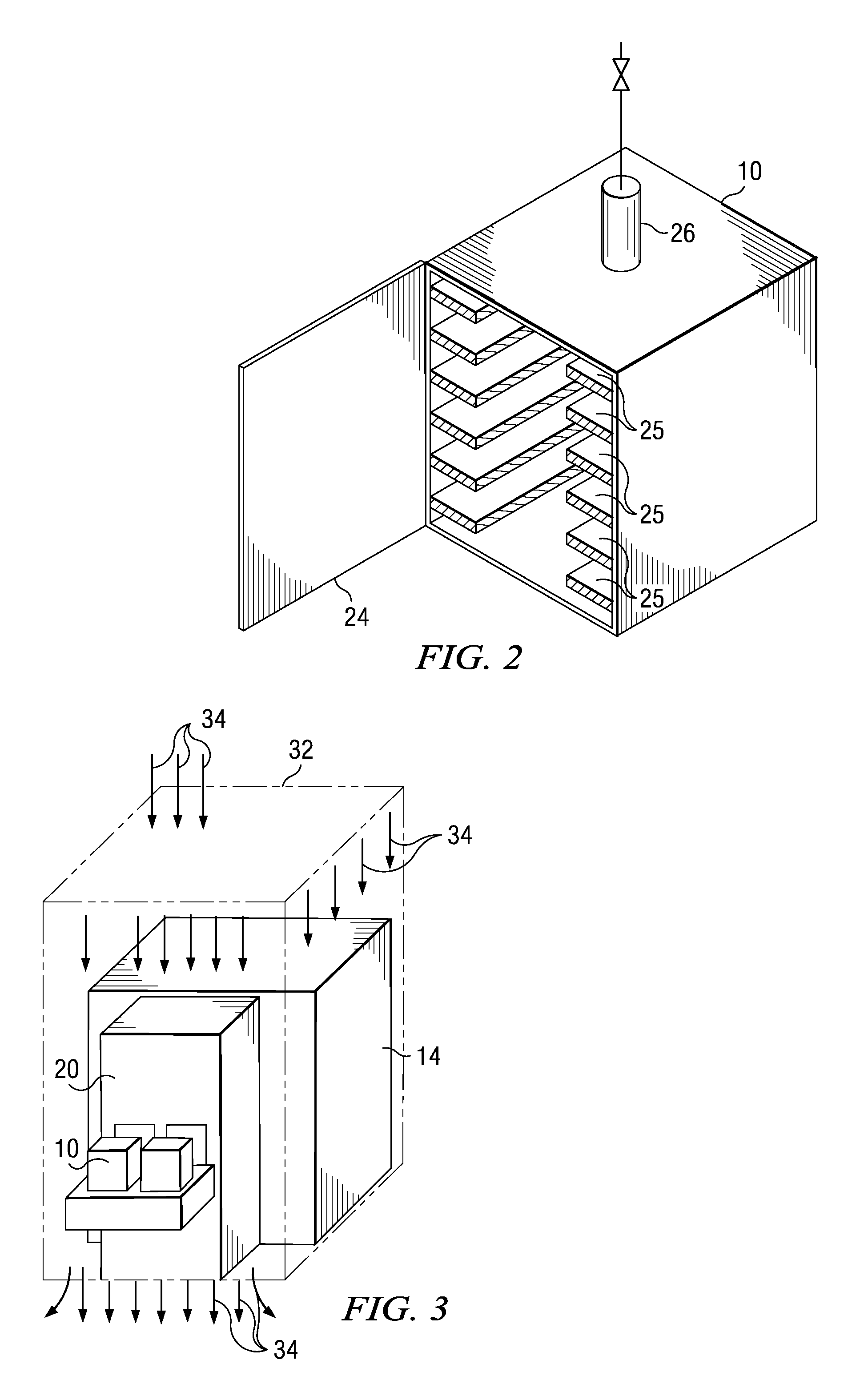
[0020]In the manufacturing processes, wafers need to go through one or more of the above-discussed tools. For example, wafer holders 10 may be transported by trolley 8 into stocker 12, which has a large wafer storage for storing wafers. Wafers holders 10 may also be transported to loa...


PUM


Abstract

A semiconductor manufacturing line includes an inert environment selected from the group consisting essentially of an inert airtight wafer holder, an inert wafer transport channel, an inert production tool, an inert clean room, and combinations thereof.

Description

[0001]This application claims the benefit of U.S. Provisional Patent Application Ser. No. 60 / 933,344, filed on Jun. 6, 2007, and entitled “Preventing Contamination in Integrated circuit Manufacturing Lines,” which application is incorporated herein by reference.TECHNICAL FIELD[0002]This invention relates generally to integrated circuits, and more particularly to the manufacturing processes and manufacturing lines of integrated circuits.BACKGROUND[0003]Existing integrated circuit (IC) manufacturing lines typically include large clean rooms and some manufacturing tools in the clean rooms, while other tools, such as metrologies and wafer transferring / transporting / exchanging paths, are within a relatively open environment. When exposed to the open environment, wafers are vulnerable to the attacks of adverse substances such as moisture, oxygen, and various airborne molecular contaminants (AMC) sources, which include etching byproduct solvents, perfumes, storage materials, chamber residua...

Claims


Application Information

Patent Timeline
IPC IPC(8): H01L21/677H01L21/44
CPCH01L21/67017H01L21/67393H01L21/67161H01L21/67703Y10S414/139
Inventor SUNG, CHIEN-MINGWANG, SIMONCHEN, JIA-RENLO, HENRYYU, CHEN-HUAWANG, JEANZUO, KEWEI
Owner TAIWAN SEMICON MFG CO LTD
Why Eureka
Try Eureka