Computer-implemented methods, carrier media, and systems for detecting defects on a wafer based on multi-core architecture

a multi-core architecture and computer-implemented technology, applied in the direction of instruments, semiconductor/solid-state device details, optical radiation measurement, etc., can solve the problems of small defects that can affect the electrical parameters of devices, the detection of defects of decreasing size has become necessary, and the defect detection of monitor wafers is not always accura

Active Publication Date: 2008-12-11
KLA TENCOR TECH CORP
View PDF9 Cites 30 Cited by
  • Summary
  • Abstract
  • Description
  • Claims
  • Application Information

AI Technical Summary

Benefits of technology

[0032]FIG. 7 is a block diagram illustrating one embodiment of a carrier medium that includes program instructions executable on a computer system for performing one or more of the computer-implemented methods described herein; and

Problems solved by technology

However, as the dimensions of semiconductor devices decrease, inspection becomes even more important to the successful manufacture of acceptable semiconductor devices because smaller defects can cause the devices to fail.
For instance, as the dimensions of semiconductor devices decrease, detection of defects of decreasing size has become necessary since even relatively small defects may cause unwanted aberrations in the semiconductor devices.
Although inspection of unpatterned wafers, or “monitor wafers,” which have been run through a process tool, may be used as a gauge for the number and types of defects that may be found on patterned wafers, or “product wafers,” defects detected on monitor wafers do not always accurately reflect the defects that are detected on patterned wafers after the same process in the same process tool.
In addition, smaller defects can have an impact on the electrical parameters of the device as the design rules shrink, which drives more sensitive inspections.
Therefore, as design rules shrink, the population of potentially yield relevant defects detected by inspection grows dramatically, and the population of nuisance defects detected by inspection also increases dramatically.
Therefore, more and more defects may be detected on the wafers, and correcting the processes to eliminate all of the defects may be difficult and expensive.
Process variation has been known for a long time to be a limiting factor of inspection sensitivity.
A controllable variation may become uncontrollable as device scaling reaches a certain point.
In particular, background noise from both types of process variation will decrease the signal-to-noise of defects in inspection output, which can prevent the detection of relatively small defects, thereby reducing the sensitivity of the inspection.

Method used


Image

  • Computer-implemented methods, carrier media, and systems for detecting defects on a wafer based on multi-core architecture
  • Computer-implemented methods, carrier media, and systems for detecting defects on a wafer based on multi-core architecture
  • Computer-implemented methods, carrier media, and systems for detecting defects on a wafer based on multi-core architecture

Examples


Embodiment Construction

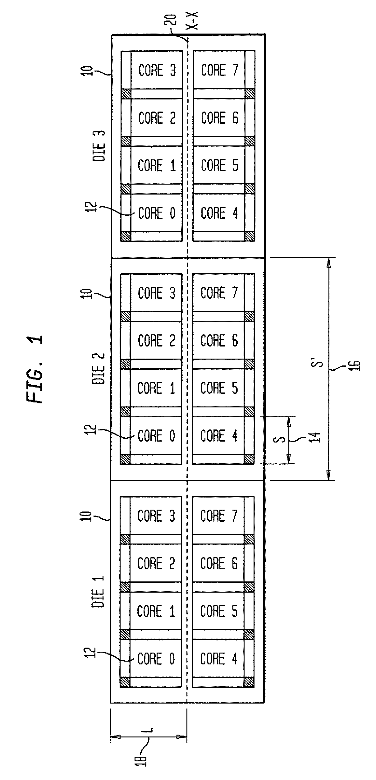
[0035]As used herein, the term “wafer” generally refers to substrates formed of a semiconductor or non-semiconductor material. Examples of such a semiconductor or non-semiconductor material include, but are not limited to, monocrystalline silicon, gallium arsenide, and indium phosphide. Such substrates may be commonly found and / or processed in semiconductor fabrication facilities. One or more layers may be formed upon a wafer. For example, such layers may include, but are not limited to, a resist, a dielectric material, a conductive material, and a semiconductive material. Many different types of such layers are mown in the art, and the term wafer as used herein is intended to encompass a wafer on which all types of such layers may be formed.

[0036]One or more layers formed on a wafer may be patterned or unpatterned. For example, a wafer may include a plurality of dies, each having repeatable patterned features. Formation and processing of such layers of material may ultimately resul...


PUM


Abstract

Computer-implemented methods, carrier media, and systems for detecting defects on a wafer based on multi-core architecture are provided. One computer-implemented method for detecting defects on a wafer includes acquiring output for the wafer generated by an inspection system. Dies are formed on the wafer, and multiple cores are formed in the dies. The method also includes detecting defects on the wafer by comparing the output for a first of the multiple cores to the output for a second of the multiple cores. The first and second of the multiple cores are formed in the same die, different dies, or the same die and different dies.

Description

BACKGROUND OF THE INVENTION[0001]1. Field of the Invention[0002]This invention generally relates to computer-implemented methods, carrier media, and systems for detecting defects on a wafer based on multi-core architecture. Certain embodiments relate to detecting defects on a wafer by comparing output generated by an inspection system for a first of multiple cores to output generated by the inspection system for a second of the multiple cores, which is formed in the same die, different dies, or the same die and different dies on the wafer as the first of the multiple cores.[0003]2. Description of the Related Art[0004]The following description and examples are not admitted to be prior art by virtue of their inclusion in this section.[0005]Fabricating semiconductor devices such as logic and memory devices typically includes processing a substrate such as a semiconductor wafer using a large number of semiconductor fabrication processes to form various features and multiple levels of th...

Claims


Application Information

Patent Timeline
Patent Type & Authority Applications(United States)
IPC IPC(8): G06F19/00
CPCG06T7/0004
Inventor ZHONG, LEIMCCORMACK, JOHN
Owner KLA TENCOR TECH CORP
Why Eureka
Try Eureka