Multi-core SoC architecture design method supporting multi-task parallel execution

An architecture design, multi-task technology, applied in the fields of electronic engineering and computer science, can solve the problems of restricting the development of high integration and miniaturization of UAVs, unable to truly improve data parallel processing, and reduce the real-time performance of data processing. High integration, improve data collection efficiency, and improve real-time effects

Inactive Publication Date: 2016-01-20
BEIHANG UNIV
View PDF6 Cites 18 Cited by
  • Summary
  • Abstract
  • Description
  • Claims
  • Application Information

AI Technical Summary

Problems solved by technology

[0003] The several airborne data processing methods mentioned above all have great shortcomings: ARM and DSP are traditional serial processors, which are not suitable for occasions that require high real-time performance. Although FPGA has a high degree of parallelism, However, its parallelism is completely at the expense of its own internal logic resources. A not very complicated algorithm is likely to occupy most of the hardware resources inside the FPGA; whether it is independent The module is still a module array, and the data communication between them is an off-chip bus communication method with a large delay, which seriously reduces the real-time performance of data processing; ARM modules are often single-core, and multiple Thread programming cannot really improve the ability of data parallel processing, because for a single-core CPU, multi-threading reflects at the micro level that each thread is processed by the CPU time-sharing with the rotation of the time slice, and it is still serial; special-purpose computers The size and weight of the UAV make it unsuitable for the design of airborne control systems, and the large number of control modules also seriously limits the development of UAVs in the direction of high integration and miniaturization.

Method used


Image

  • Multi-core SoC architecture design method supporting multi-task parallel execution
  • Multi-core SoC architecture design method supporting multi-task parallel execution

Examples


Embodiment Construction

[0028] Combine below Attached picture The present invention is described in further detail.

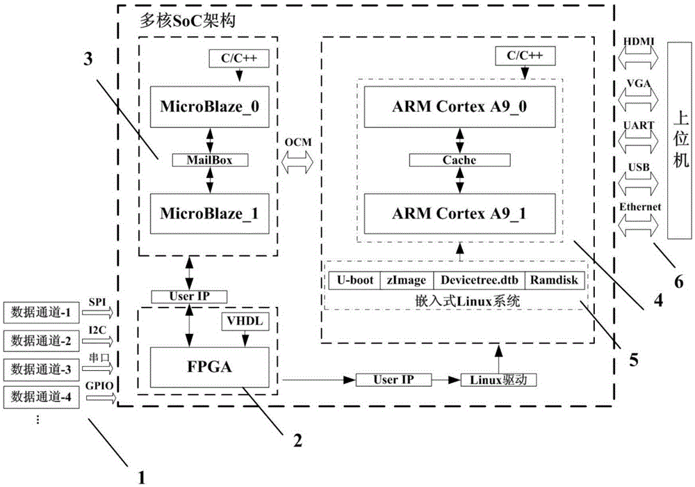
[0029] System Structure Box Figure such as figure 1 As shown, the present invention relates to a multi-core SoC architecture design method that supports multi-task parallelism. By building a multi-core architecture inside the SoC chip, it has multi-task parallel processing capabilities. Compared with the prior art, the present invention can not only significantly improve The real-time nature of data parallel acquisition, processing, output and inter-core interaction can significantly promote the development of UAVs towards high integration and miniaturization. The SoC chip model mentioned is xc7z020clg484-1 of Xilinx Company.

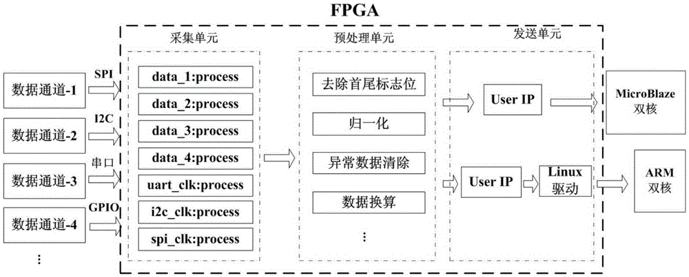
[0030] (1) attached figure 1 Module 1 is the parallel acquisition of multi-channel data. In order to collect data from devices with different interfaces (SPI, I2C, serial port and GPIO interface), module 2 first designed the clocks of these four interf...


PUM


Abstract

The invention relates to a multi-core SoC architecture design method supporting multi-task parallel execution. The method mainly comprises: establishing a MicroBlaze dual-core module and an ARM dual-core module; designing a multi-core multi-thread based multi-task parallel execution module based on the established MicroBlaze dual-core module and the ARM dual-core module; and meanwhile, designing a hardware acceleration module based on an FPGA. According to the multi-core SoC architecture design method, external multi-channel data are collected simultaneously through the FPGA, and then multi-channel data are transmitted to different cores for parallel execution, wherein the FPGA is designed in a mode that the FPGA interacts with MicroBlaze dual cores through User-IP, the FPGA interacts with ARM dual cores through the User-IP and a Linux driving module, the MicroBlaze dual cores interact through MailBox, the ARM dual cores interact through Cache, and the MicroBlaze dual cores and the ARM dual cores interact through OCM; and by establishing a multi-core SoC architecture, the parallel execution of multiple tasks on multiple cores can be realized, so that the executing efficiency of the multiple tasks is greatly improved.

Description

technical field [0001] The present invention belongs to the fields of electronic engineering and computer science. The present invention specifically relates to a multi-core SoC architecture design method supporting multi-task parallelism, aiming at realizing the parallel execution of multi-tasks on multi-cores by constructing a multi-core SoC architecture, so as to improve the execution efficiency of multi-tasks. Background technique [0002] With the research and application of UAV technology and its equipment, how to further improve the performance of UAV airborne control system is very necessary. The UAV airborne control system mainly includes an inertial navigation module, a GPS / Beidou navigation module, a terrain matching navigation module, and the collection and calculation of various parameters. At present, the commonly used method for processing these data is: design many independent control modules, such as ARM module to complete image processing, DSP module to co...

Claims


Application Information

Patent Timeline
Patent Type & Authority Applications(China)
IPC IPC(8): G06F9/38G06F15/16
Inventor 陶飞邹孝付张霖
Owner BEIHANG UNIV
Why Eureka
Try Eureka