Structure of packaging substrate having capacitor embedded therein and method for fabricating the same

a technology of packaging substrate and capacitor, which is applied in the direction of lithography/patterning, printed capacitor incorporation, conductive pattern formation, etc., can solve the problems of unfavorable shrinkage of package size, restricted flexibility of wiring layout on the surface, and increased noise, so as to avoid the formation of voids, improve the flexibility of passive component layout, and save materials

Inactive Publication Date: 2008-12-18
PHOENIX PRECISION TECH CORP
View PDF2 Cites 5 Cited by
  • Summary
  • Abstract
  • Description
  • Claims
  • Application Information

AI Technical Summary

Benefits of technology

[0013]The packaging substrate structure having capacitors embedded therein can save production a lot of high dielectric material, avoid the formation of voids, and reduce the parasitic capacitance between the circuits.
[0018]The present invention can enhance the flexibility of layout of passive components and the circuit in the packaging substrate, as well as the usable surface area of the packaging substrate to meet the requirement of miniaturization.
[0019]In addition, the process of the present invention, fabricating a capacitor on the metal plate and then utilizing conductive vias or through holes for electro-connections, can save materials, avoid the formation of voids and poor uniformity of thickness, reduce the parasitic capacitance between the circuits, and simplify the process.

Problems solved by technology

However, as the density of wiring in a package structure increases, the noise also increases.
In conventional methods, utilizing surface mount technology (SMT) integrates most passive components onto a surface of a packaging substrate, such that the flexibility of wiring layout on the surface is restricted, and the occupied space is unfavorable to shrinkage of package size.
However, the prior art forms a whole piece of high dielectric material layer within a packaging substrate, wherein the used part of the high dielectric material layer for a capacitor is merely the one between the inner electrode plate and the outer electrode plate, while the unused part of the high dielectric material layer electrically contacts with the circuits, such that the structure has several drawbacks: first, the unused part of the high dielectric material layer causes waste, unfavorable to reduce the cost; second, owing to the poor fluidity of the high dielectric material, voids and poor uniformity of thickness occur; third, the unused part of the high dielectric material layer electrically contacts the circuits, so that parasitic capacitance occurs to interfere with electrical qualities; finally, because the electrode plates and the circuits are laid together in a circuit layer, such that the flexibility of layouts of both the electrode plates and the circuits is compromised.

Method used


Image

  • Structure of packaging substrate having capacitor embedded therein and method for fabricating the same
  • Structure of packaging substrate having capacitor embedded therein and method for fabricating the same
  • Structure of packaging substrate having capacitor embedded therein and method for fabricating the same

Examples


Embodiment Construction

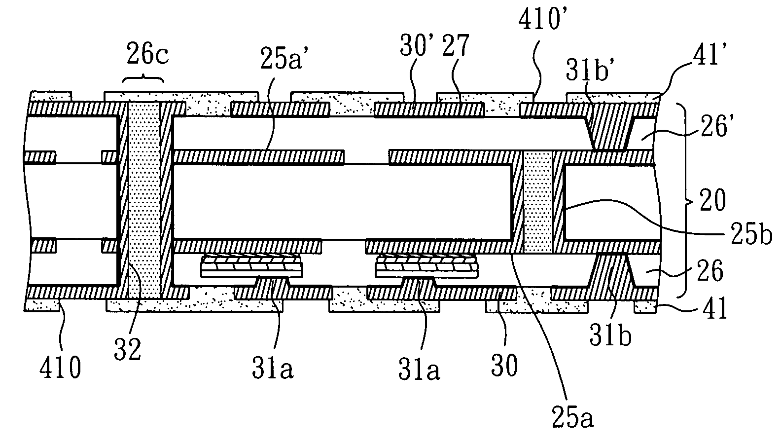
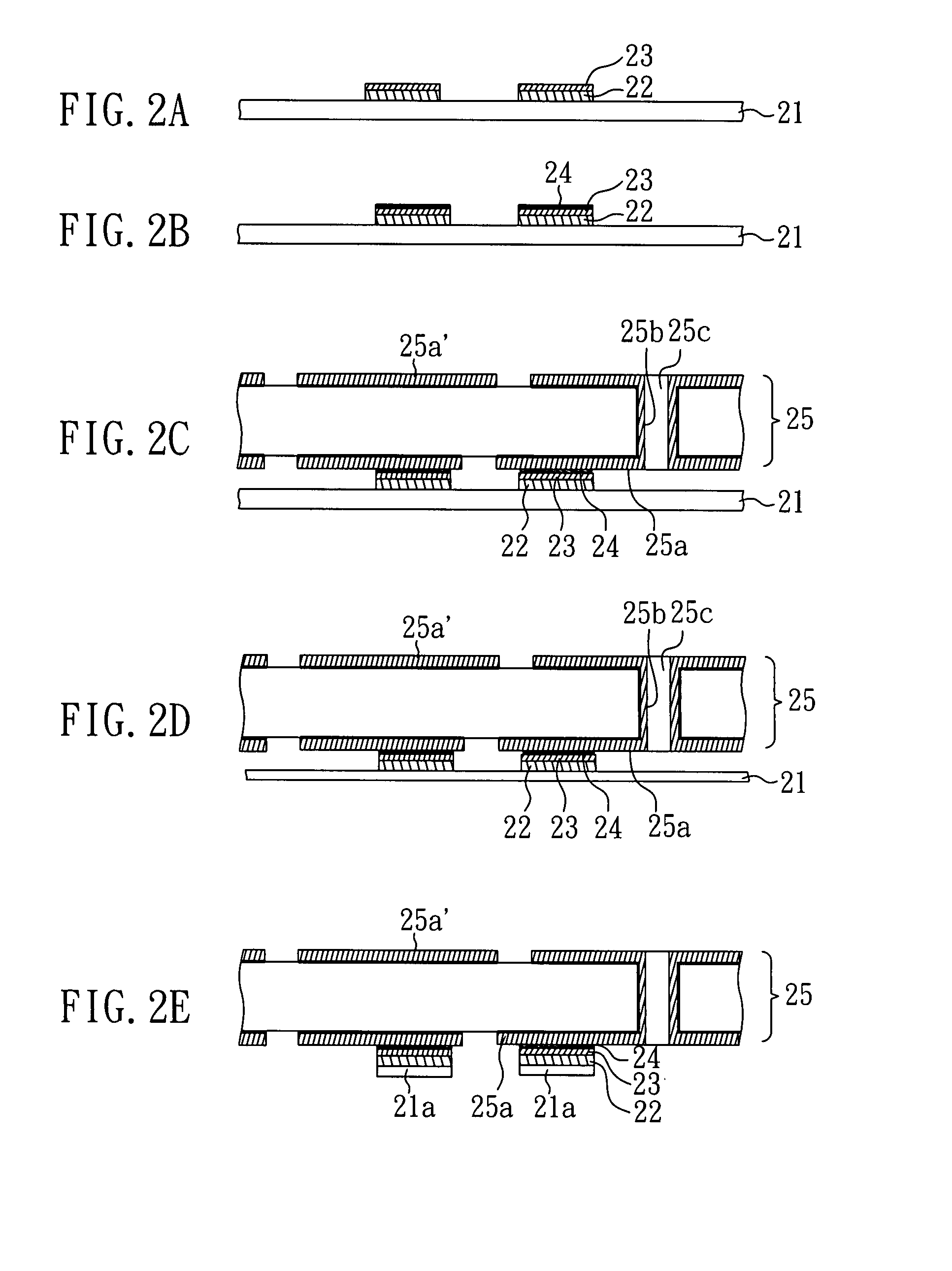
[0023]FIG. 2H is a cross-section view of a structure of the present invention about a packaging substrate having capacitors embedded therein. As shown in FIG. 2H, the semiconductor packaging substrate comprises an core substrate 25, two dielectric layers 26,26′, and outer circuit layer 30,30′. The core substrate 25 has inner circuit layers 25a,25a′ made of copper on two surfaces of the core substrate 25. The core substrate 25 can further comprise an inner plated through hole 25b so as to connect the inner circuit layers 25a,25a′. The dielectric layers 26,26′ are disposed on two sides of the core substrate 25, and the material of the dielectric layer 26, 26′ is selected from the group consisting of a non-photosensitive organic resin, a photosensitive organic resin (e.g. ABF (Ajinomoto Build-up Film), BCB (Benzocyclo-buthene), LCP (Liquid Crystal Polymer), PI (Poly-imide), PPE (Poly(phenylene ether)), PTFE (Poly (tetra-fluoroethylene)), FR4, FR5, BT (Bismaleimide Triazine), or Aramide...


PUM

PropertyMeasurementUnit
structureaaaaaaaaaa
dielectricaaaaaaaaaa
dielectric coefficientaaaaaaaaaa

Abstract

A structure of a packaging substrate having capacitors embedded therein is disclosed. The structure comprises a core substrate, a dielectric layer, and an outer circuit layer. The core substrate comprises an inner circuit layer. The dielectric layer is disposed at both sides of the core substrate, having first conductive vias each connecting to the inner circuit layer through a piece of outer electrode plate, a piece of high dielectric material layer, a piece of inner electrode plate, and a piece of adhesive layer, in sequence. The outer circuit layer is disposed on the surface of each of the dielectric layers. Herein, the capacitor is composed of a piece of the outer electrode plate, the high dielectric material layer and the inner electrode plate. The invention further comprises a method for manufacturing the same. This can achieve low costs, avoid the formation of voids, and reduce parasitic capacitance.

Description

BACKGROUND OF THE INVENTION[0001]1. Field of the Invention[0002]The present invention relates to a structure of a packaging substrate having capacitors embedded therein and a method for fabricating the same, which can reduce the parasitic capacitance, avoid the formation of voids and poor uniformity of thickness resulted from the high dielectric material layer of prior art.[0003]2. Description of Related Art[0004]Currently, the relentless progress in semiconductor fabricating process and electronic functions of microelectronic devices has lead to a highly integrated development of semiconductor chips. Quantity of input / output terminals and density of wiring in package structures increase as semiconductor chips develop toward high integration. However, as the density of wiring in a package structure increases, the noise also increases. Generally, in order to obviate noise or compensate electricity, passive components, e.g. resistors, capacitors, and inductors, are installed in a semi...

Claims


Application Information

Patent Timeline
Patent Type & Authority Applications(United States)
IPC IPC(8): H05K1/16H05K3/10
CPCH05K1/162H05K3/4644H05K3/4652H05K2201/0355H05K2201/09509Y10T29/49155H05K2203/0152H05K2203/0353H05K2203/0376H05K2203/0537H05K2203/1131H05K2201/09763
Inventor LIEN, CHUNG-CHENGYANG, CHIH-KUI
Owner PHOENIX PRECISION TECH CORP
Why Eureka
Try Eureka