

Dielectric layer and thin film transistor
a thin film transistor and dielectric layer technology, applied in the direction of solid-state devices, basic electric elements, insulation bodies, etc., can solve the problems of deteriorating electrical characteristics, increasing the number of particles being confined within the gate insulation layer, and it is rather difficult to further improve the electrical characteristics of the polysilicon tft during the conventional polysilicon tft fabricating process, so as to achieve superior electrical characteristics
- Summary
- Abstract
- Description
- Claims
- Application Information
AI Technical Summary
Benefits of technology
Problems solved by technology
Method used
Image

Examples
first embodiment
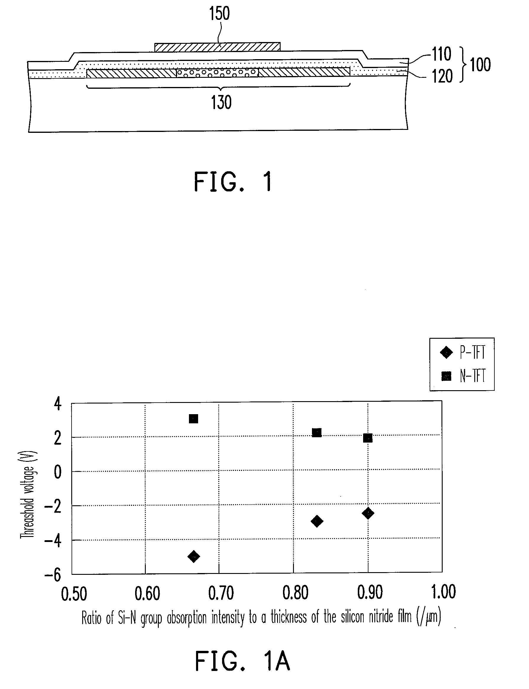
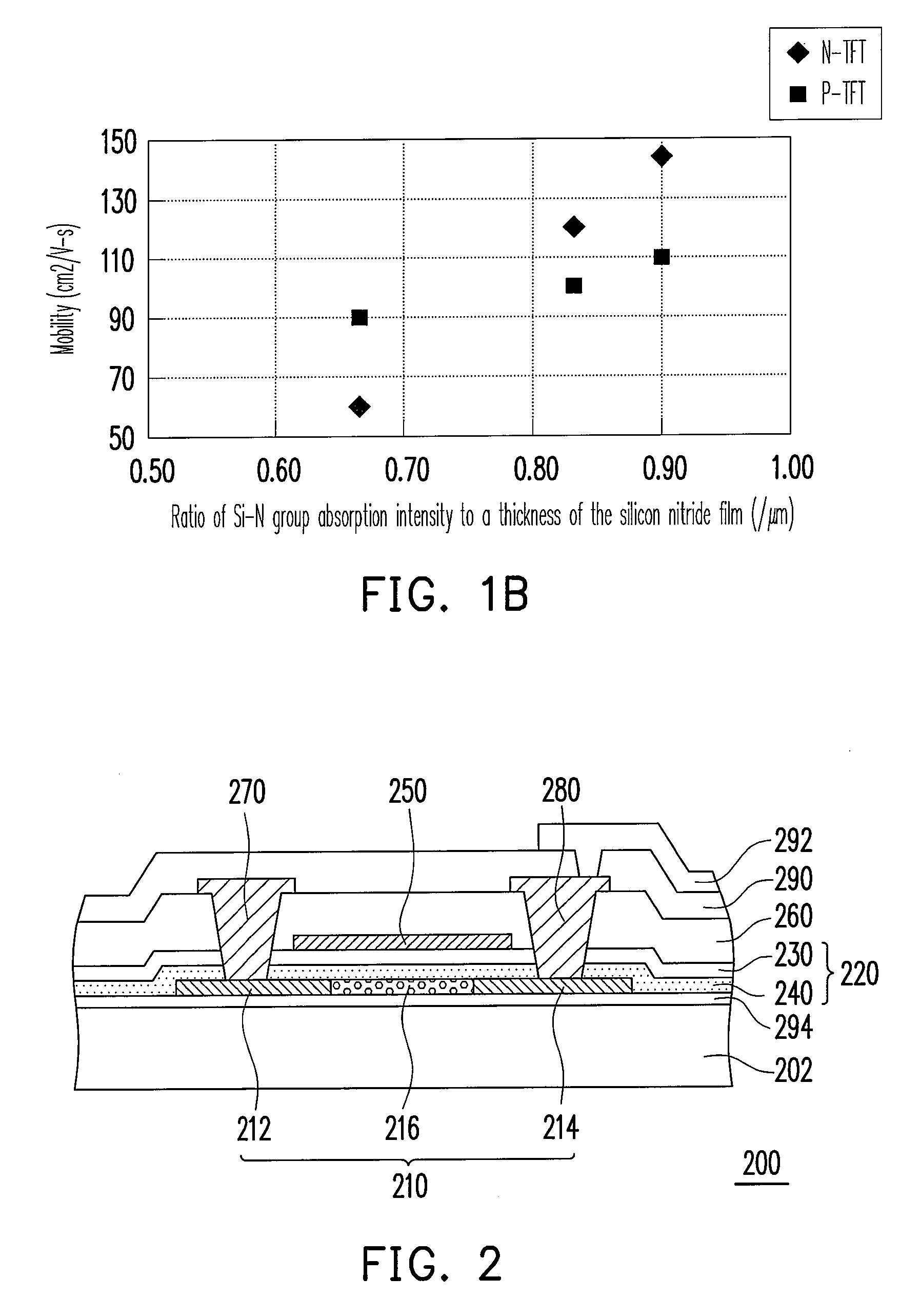
[0025]FIG. 1 is a schematic view of a dielectric layer of the present invention applied in a TFT. Referring to FIG. 1, a dielectric layer 100 including a film with silicon compound contain oxygen 120 and a film with silicon compound contain nitrogen 110. In the present embodiment of the invention, the film with silicon compound contain oxygen is a silicon oxygen film and the film with silicon compound contain nitrogen is a silicon nitride film is used as an example, but not limited it. In the present embodiment, the film with silicon compound contain nitrogen 110 are formed by a chemical vapor deposition (CVD) process by using a nitrogen-based gas, such as N2O, and a silicon-based gas, such as SiH4, as reactive gases. The present embodiment is not limited to the reactive gases recited herein. Other reactive gases may be optionally used, specifically, the nitrogen-based gases may be nitrogen, ammonia, a gas / ammonia mixture, a nitrogen / N2O mixture, N2O, other gases, or any mixture of ...
second embodiment
[0030]The embodiment provides a TFT 200 including a substrate 202, an active layer 210, a first dielectric layer 220, a gate 250, a second dielectric layer 260, a source region 212 / drain region 214, a third dielectric layer 290 and a pixel electrode 292. The active layer 210 is disposed on the substrate 202. The active layer 210 has a source region 212, a drain region 214 and a channel region 216 located between the source region 212 and the drain region 214. The first dielectric layer 220 is disposed on the substrate 202 to cover the active layer 210. The gate 250 is disposed on a portion of the first dielectric layer 220. The second dielectric layer 260 is disposed on the substrate 202 to cover the gate 250. The source 270 / drain 280 is disposed on a portion of the second dielectric layer 260 and electrically connected to the source region 212 / drain region 214 of the active layer 210. The third dielectric layer 290 is disposed on the substrate 202 to cover the source 270 / drain 280....
third embodiment
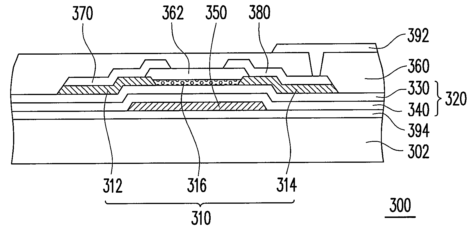
[0036]FIG. 3 is a schematic view illustrating another TFT of the present invention. Referring to FIG. 3, a TFT 300 includes a substrate 302, a gate 350, a first dielectric layer 320, an active layer 310, a source 370 / drain 380, a second dielectric layer 360, and a pixel electrode 392. The gate 350 is disposed over a substrate 302. The first dielectric layer 320 is disposed over the substrate 302 to cover the gate 350. The active layer 310 is disposed on a portion of the first dielectric layer 320. The active layer 310 has a source region 312, a drain region 314, and a channel region 316 located between the source region 312 and the drain region 314. The source 370 / drain 380 is electrically connected to the source region 312 / drain region 314 of the active layer 310. The second dielectric layer 360 is disposed over the substrate 302 to cover the source 370 / drain 380, the active layer 310 and the first dielectric layer 320. The pixel electrode 392 is disposed on a portion of the second...
PUM
 Abstract
Description
Claims
Application Information