Transimpedance Amplifier

a technology of transimpedance amplifier and amplifier, which is applied in the direction of amplification control details, gain control, electromagnetic transceivers, etc., can solve problems such as waveform distortion

Active Publication Date: 2008-12-18
NIPPON TELEGRAPH & TELEPHONE CORP +1
View PDF2 Cites 45 Cited by
  • Summary
  • Abstract
  • Description
  • Claims
  • Application Information

AI Technical Summary

Benefits of technology

[0026]According to the present invention, gain switching signals are output to the first and second transimpedance amplifier core circuits on the basis of the result obtained by comparing / determining a comparative input voltage as a differential output signal from the inter-stage buffer circuit with the first hysteresis characteristic, thereby performing the gain switching operation of switching the gains of the respective circuits. The present invention uses a hysteresis characteristic for determining on the basis of a comparative input voltage whether it is necessary to switch the gains, and hence need not hold any comparative input voltage for gain switching determination by using a level holding circuit with a slow response time. This makes it possible to instantaneously perform gain switching determination on the basis of a comparative input voltage which changes in accordance with an input current and achieve instantaneous response corresponding to burst data.

Problems solved by technology

In a transimpedance amplifier of this type, as the input current Iin increases, the amplitude of the output voltage Vout saturates, resulting in waveform distortion.

Method used


Image

  • Transimpedance Amplifier
  • Transimpedance Amplifier
  • Transimpedance Amplifier

Examples


first embodiment

[0114]The arrangement of a transimpedance amplifier according to the first embodiment of the present invention will be described with reference to FIGS. 1 and 2.

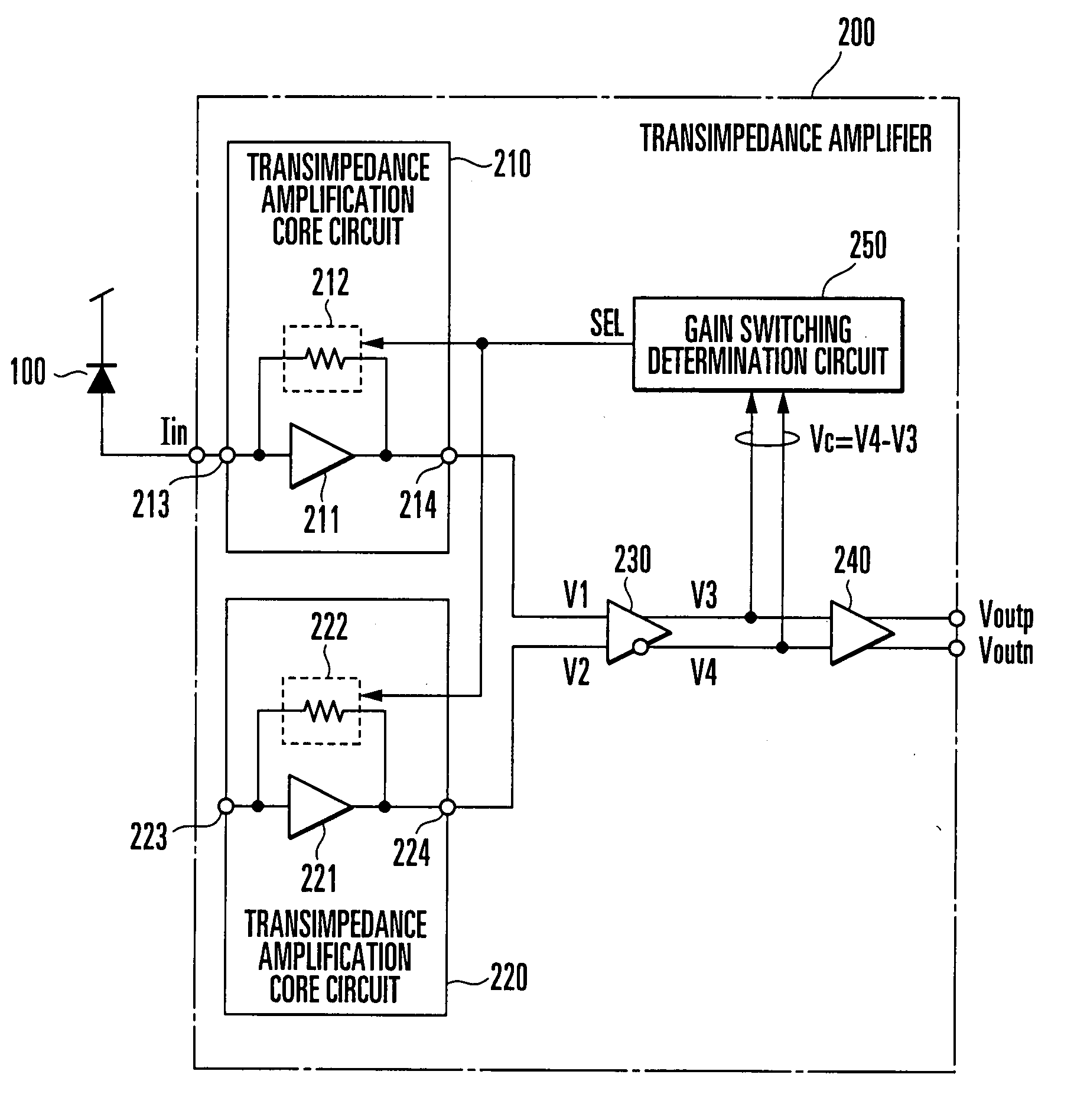
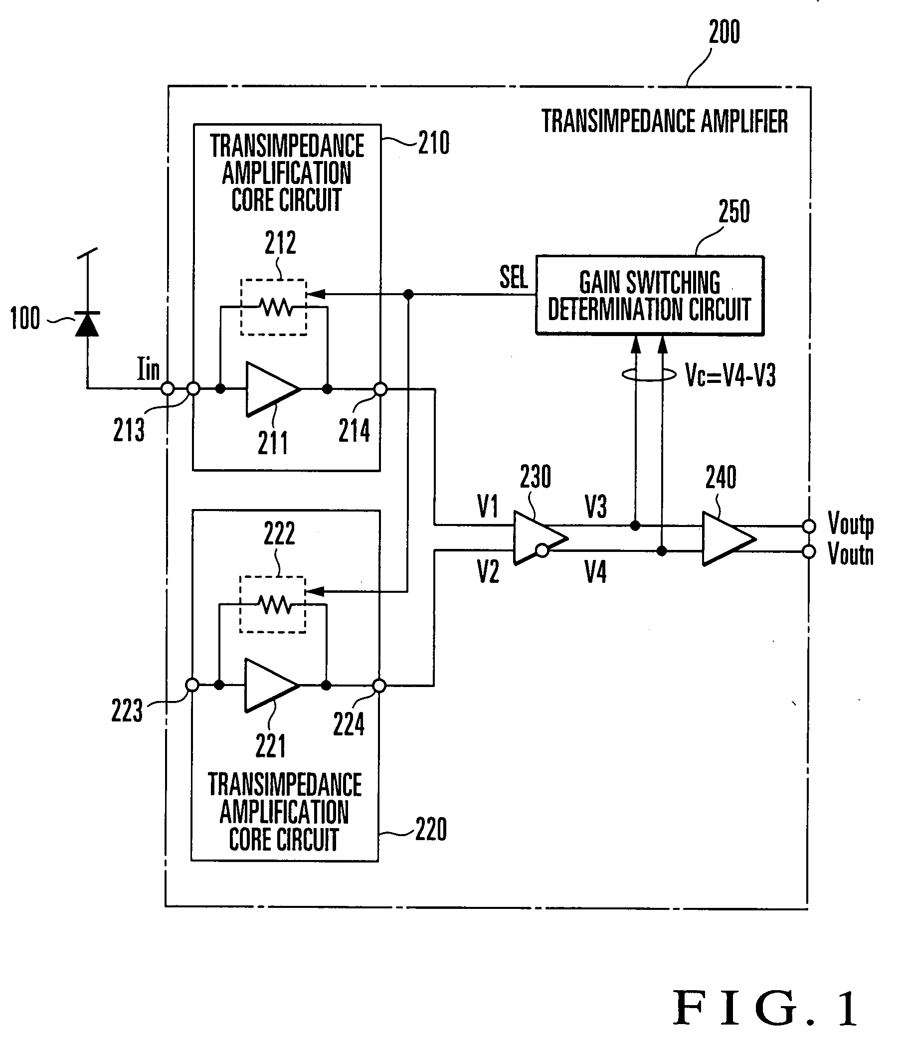
[0115]In an optical transmission circuit such as an optical transmission system, optical interconnection, or passive optical network (OPN) system which can perform high-speed data transmission, an optical reception circuit which converts an optical signal received by a light-receiving element 100 and sent through an optical fiber into an electrical signal uses a transimpedance amplifier 200 shown in FIG. 1.

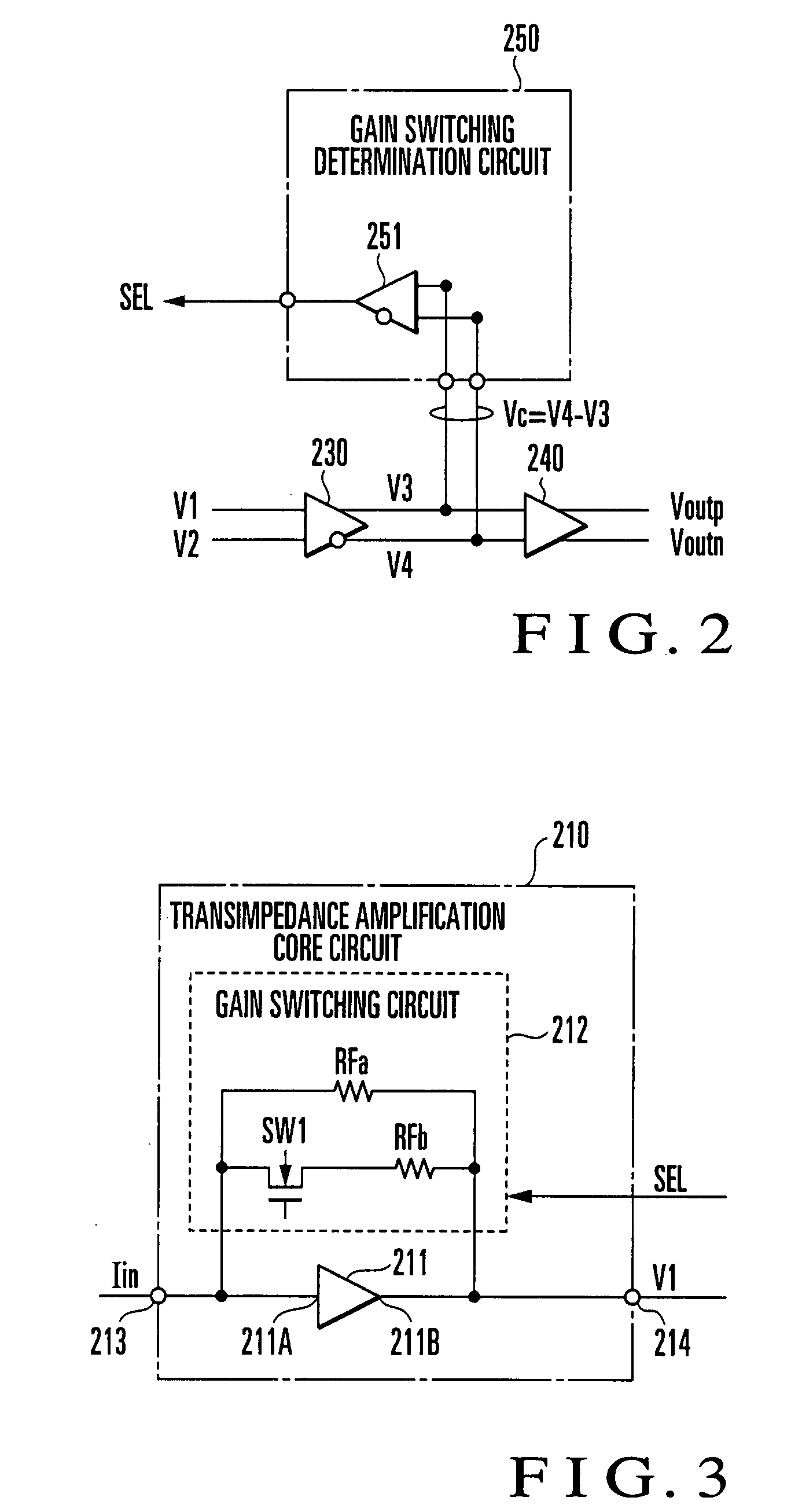
[0116]As shown in FIG. 1, the transimpedance amplifier 200 mainly comprises a first transimpedance amplifier core circuit 210, second transimpedance amplifier core circuit 220, inter-stage buffer circuit 230, output buffer circuit 240, and gain switching determination circuit 250.

[0117]The first transimpedance amplifier core circuit 210 includes an amplification circuit 211, gain switching circuit 212, input terminal 213, ...

second embodiment

[0151]The arrangement of a transimpedance amplifier according to the second embodiment of the present invention will be described next with reference to FIGS. 9 to 11. The same reference numerals as in FIGS. 2 to 4 denote the same components in FIGS. 9 to 11.

[0152]The first embodiment has exemplified the case wherein the gains of the transimpedance amplifier core circuits 210 and 220 are switched by one step between “high gain” and “low gain”. The second embodiment will exemplify a case wherein gains are switched by a plurality of steps, more specifically, a case wherein the gains of transimpedance amplifier core circuits 210 and 220 are switched by two steps between “high gain”, “intermediate gain”, and “low gain”. Note that the constituent elements of the transimpedance amplifier according to this embodiment are the same as those in the first embodiment except for a gain switching determination circuit and first and second transimpedance amplifier core circuits, and a detailed des...

third embodiment

[0171]A concrete example of a transimpedance amplifier core circuit used in a transimpedance amplifier according to the third embodiment of the present invention will be described next with reference to FIGS. 14 to 16.

[0172]Each of transimpedance amplifier core circuits 210B and 220B in FIG. 14 includes a transimpedance gain switching circuit 281 which switches transimpedance gains and an open loop gain switching circuit 282 which switches open loop gains as each of gain switching circuits 212B and 222B which switches the gains in two steps between “high gain”, “intermediate gain”, and “low gain”.

[0173]The transimpedance gain switching circuit 281 comprises feedback resistors RF1, RF2, and RF3 which determine a transimpedance gain and NMOS transistors NM1 and MN2 which operate as switches. The open loop gain switching circuit 282 comprises load resistors RL1, RL2, and RL3 which determine an open loop gain and NMOS transistors MN3 and MN4 which operate as switches. The NMOS transisto...


PUM


Abstract

A gain switching determination circuit (250) compares / determines a comparative input voltage (Vc) from an inter-stage buffer (230) with a first hysteresis characteristic, and outputs a gain switching signal (SEL) based on the comparison / determination result to first and second transimpedance amplifier core circuits (210, 220), thereby switching the gains of the core circuits. This obviates holding a comparison input voltage with long response time in a level holding circuit for gain switching determination, which allows instantaneous gain switching determination and instantaneous response corresponding to burst data.

Description

TECHNICAL FIELD[0001]The present invention relates to a transimpedance amplifier which receives a current signal obtained by photoelectric conversion using a light-receiving element and converts / amplifies the signal into a voltage signal in an optical reception circuit and, more particularly, to a transimpedance amplifier which can cope with an input current with a large dynamic range.BACKGROUND ART[0002]In an optical transmission circuit in an optical transmission system, optical interconnection, passive optical network (to be referred to as a PON (Passive Optical Network) hereinafter) system, or the like which can perform high-speed data transmission, an optical reception circuit which converts an optical signal into an electrical signal uses a transimpedance amplifier.[0003]A transimpedance amplifier receives an input current Iin obtained by photoelectrically converting a received optical signal using a light-receiving element, converts the current into an output voltage Vout by ...

Claims


Application Information

Patent Timeline
Patent Type & Authority Applications(United States)
IPC IPC(8): H03F3/45H04B10/43
CPCH03F1/08H03F3/087H03G1/0088H03G3/3084
Inventor NAKAMURA, MAKOTOUMEDA, YOHTAROENDOU, JUNAKATSU, YUJIIMSI, YUUKITOBAYASHI, MASATOSHIURABE, YOSHIKAZUIIZUKA, HATSUSHIHYODO, EIJI
Owner NIPPON TELEGRAPH & TELEPHONE CORP
Why Eureka
Try Eureka