Electron beam inspection method and electron beam inspection apparatus

a technology of electron beam and inspection method, which is applied in the direction of optical radiation measurement, instruments, therapy, etc., can solve the problems of degrading the sensitivity of detecting defects or foreign objects, inability to apply conventional charging cancellation methods using ultraviolet rays, and inability to achieve positive charging within the range of detection range, etc., to achieve high detection range and high speed

Inactive Publication Date: 2008-12-25
HITACHI LTD
View PDF15 Cites 37 Cited by
  • Summary
  • Abstract
  • Description
  • Claims
  • Application Information

AI Technical Summary

Benefits of technology

[0030]According to the present invention, positive charging derived from ultraviolet irradiation and negative charging occurring during imaging of reflected electrons can be well balanced. Negative cha...

Problems solved by technology

This poses a problem in that the sensitivity in detecting a defect or foreign matter is degraded.
However, the conventional charging cancellation method employing ultraviolet rays cannot be applied for reasons described below.
First, in the conventional method, means for observing an irradiated area of ultraviol...

Method used


Image

  • Electron beam inspection method and electron beam inspection apparatus
  • Electron beam inspection method and electron beam inspection apparatus
  • Electron beam inspection method and electron beam inspection apparatus

Examples


embodiment 1

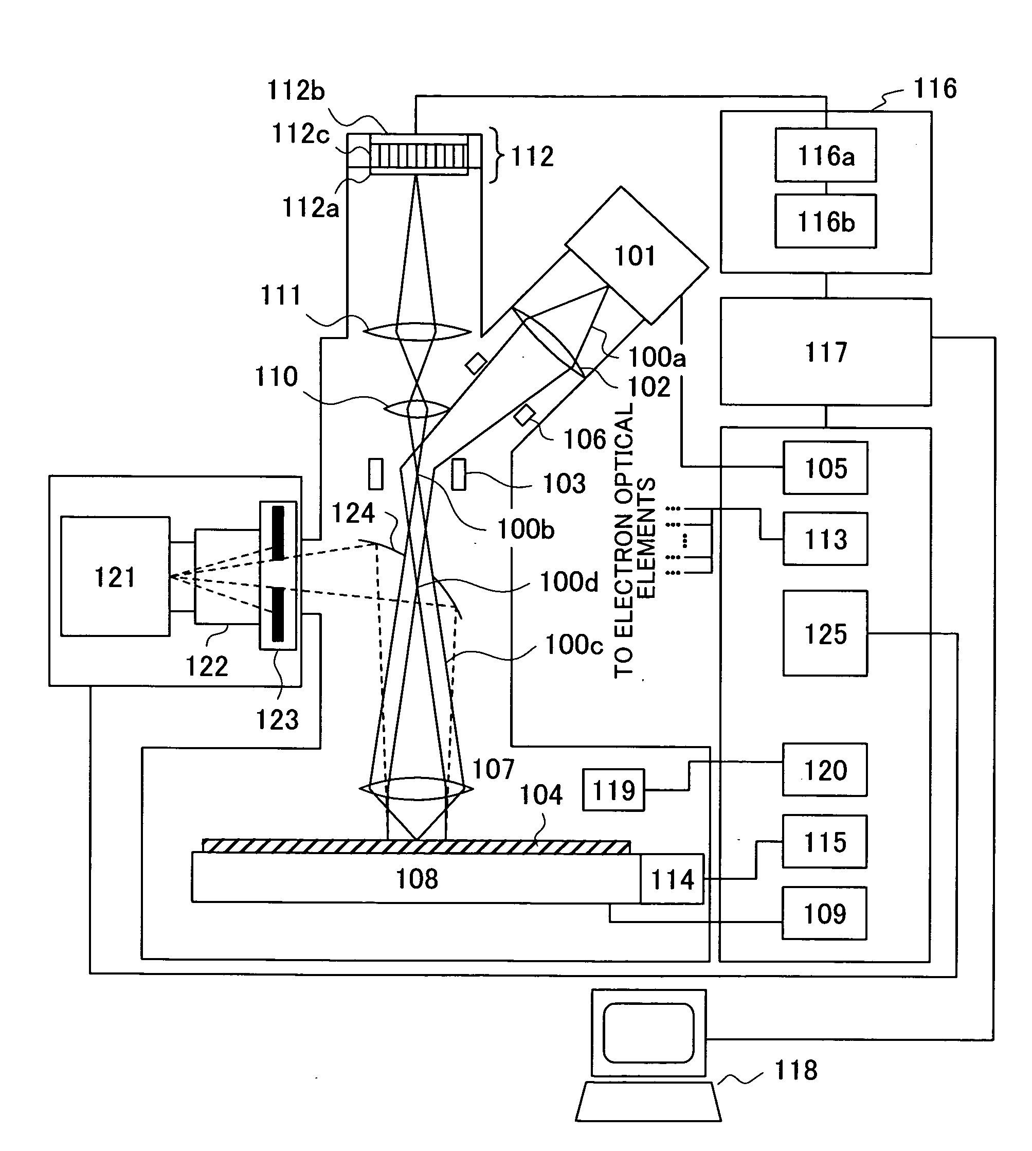
[0042]FIG. 1 shows an embodiment of a hardware configuration of a reflected-electron imaging type electron beam inspection apparatus in which the present invention is implemented. Noted is that a vacuum exhaust pump and its control unit, and an exhaust pipe are not shown in the drawing. Moreover, for convenience' sake, the ratio of dimensions is appropriately modified.

[0043]To begin with, the major elements of an electron optical system of the present apparatus will be described below. An irradiated electron beam 10a emitted from an electron gun 101 is deflected by an E×B deflector 103 while being focused by a condenser lens 102. After forming a crossover 100d, the electron beam is irradiated as a bundle of substantially parallel rays to a sample 104. In the drawing, the condenser lens 102 is drawn as one lens. Alternatively, a system having multiple electron lenses combined may be adopted in order to optimize optical conditions. As the electron gun 101, a Zr—O / W Schottky electron s...

embodiment 2

[0083]In the present embodiment, modulation of the intensity of ultraviolet rays by the ultraviolet transportation system 122 shown in FIG. 1 is achieved merely by inserting a filter. In the present embodiment, the ultraviolet light source 121 is a light source capable of feeding a sufficient amount of ultraviolet rays for the purpose of acquiring a photoelectron image.

[0084]In the ultraviolet transportation system 122 shown in FIG. 7, a filter 702 exhibiting a finite transmittance with respect to ultraviolet rays is attached to a rod 701 that can perform plunging and rising motions relative to the ultraviolet ray axis and perform rotating motion with the axis thereof as a center. Multiple filters 702 (two filters in FIG. 7) may be included. The filter 702 may have a filtering material attached to an appropriate holding structure.

[0085]When a photoelectron image is acquired, the filters 702 are withdrawn from the ultraviolet ray path by a moving mechanism. A maximum amount of light ...

embodiment 3

[0087]In the aforesaid embodiments, an operation of limiting an ultraviolet irradiation area in an electron-beam irradiation area is performed mainly by handling the pinhole on the ultraviolet ray path. However, in the present embodiment, a diaphragm for limiting a field of view is mounted on the light path of an electron beam in order to improve the precision in limiting the ultraviolet irradiation area in the electron-beam irradiation area.

[0088]FIG. 8 shows the configuration of an electron beam inspection apparatus having a diaphragm 801 mounted on the optical path of the electron optical system. In FIG. 8, the same reference numerals are assigned to components identical to those shown in FIG. 1. The description of the components will be omitted. The diaphragm 801 is mounted in an irradiation optical system for fear the presence of the diaphragm may adversely affect an imaging optical system. In the present configuration, the shape and size of an electron-beam irradiation area ar...


PUM


Abstract

An electron beam inspection apparatus images reflected electrons and cancels negative charging derived from electron-beam irradiation. Ultraviolet rays are irradiated and an irradiated area of ultraviolet rays is displayed as a photoelectron image. The photoelectron image and a reflected-electron image are displayed on a monitor while being superposed on each other, to easily grasp the positional relationship between the images and the difference in size between them. Specifically, the shape of the irradiated area of an electron beam includes the shape of the irradiated area of ultraviolet rays on a display screen. The intensity of the ultraviolet rays in the irradiated area of the electron beam is adjusted while the reflected-electron imaging conditions for the reflected-electron image are sustained. Moreover, an amount-of-ultraviolet ray adjustment mechanism is controlled on the monitor so that an amount of the ultraviolet rays is adjusted while observing a reflected-electron image obtained during ultraviolet irradiation.

Description

CLAIM OF PRIORITY[0001]The present invention claims priority from Japanese Application JP-2007-161266, filed on Jun. 19, 2007, the content of which is hereby incorporated by reference on to this application.BACKGROUND OF THE INVENTION[0002]1. Field of the Invention[0003]The present invention relates to a technology for inspecting presence or absence of a foreign matter or a defect on a sample such as a wafer or a disk medium.[0004]2. Description of the Related Art[0005]Along with a tendency toward high-density patterning of electronic devices, the minimum line width of a patterned shape included in a large-scale integration or the size of a recording bit on a magnetic disk has been reduced down to an ultramicroscopic size of 100 nm or less. The tendencies toward the ultramicroscopic designing and high-density patterning would further continue. In the process of such high-density patterning, the presence of a small foreign matter (particles or scratches) of about 10 nm in size, which...

Claims


Application Information

Patent Timeline
IPC IPC(8): G01N23/225G01J1/42
CPCG01N23/225H01J37/026H01J37/285H01J37/29H01J2237/0047H01J2237/221H01J2237/2446H01J2237/24495H01J2237/2482H01J2237/2855
Inventor HASEGAWA, MASAKIOHTA, HIROYA
Owner HITACHI LTD
Why Eureka
Try Eureka