Integrated structures and methods of fabrication thereof with fan-out metallization on a chips-first chip layer

a technology of integrated structures and chip layers, applied in the direction of printed circuit manufacturing, printed circuit aspects, cross-talk/noise/interference reduction, etc., can solve the problems of speed, size and interconnect density, conventional process speed limitations, and the inability to provide electronic packaging and interconnects which provide maximum performance. , to achieve the effect of reducing the cost of manufacturing, and improving the quality of manufacturing

Inactive Publication Date: 2008-12-25
EPIC TECH INC
View PDF36 Cites 96 Cited by
  • Summary
  • Abstract
  • Description
  • Claims
  • Application Information

AI Technical Summary

Benefits of technology

[0009]Briefly summarized, this invention comprises, in a first aspect, an electronic module which includes: a chip layer including at least one chip comprising at least one side surface, an upper surface, a lower surface, at least one contact pad at the upper surface, and a pad mask over the upper surface with at least one opening therein exposing the at least one contact pad at the upper surface; a structural material surrounding and physically contacting the at least one side surface of each chip of the at least one chip of the chip layer, the structural material having an upper surface substantially co-planar with or parallel to an upper surface of the at least one chip, and defining at least a portion of a front surface of the chip layer, and a lower surface sub...

Problems solved by technology

In recent years, this approach has met with problems of speed, size and interconnect density due to ever-constant demands for reduced size and increased performance from such integrated circuit packages.
Process speed is conventionally limited by the fact that individual packages have loading capacitance and inductance associated with their relatively long pins and by the large size of conductor runs in the packages relative to the size of the conductors of a bare IC chip.
As the speed of computers and other devices continues to increase, the problem of providing electronic packaging and interconnect which provides maximum performance has become a significant challenge.
One problem w...

Method used


Image

  • Integrated structures and methods of fabrication thereof with fan-out metallization on a chips-first chip layer
  • Integrated structures and methods of fabrication thereof with fan-out metallization on a chips-first chip layer
  • Integrated structures and methods of fabrication thereof with fan-out metallization on a chips-first chip layer

Examples


Embodiment Construction

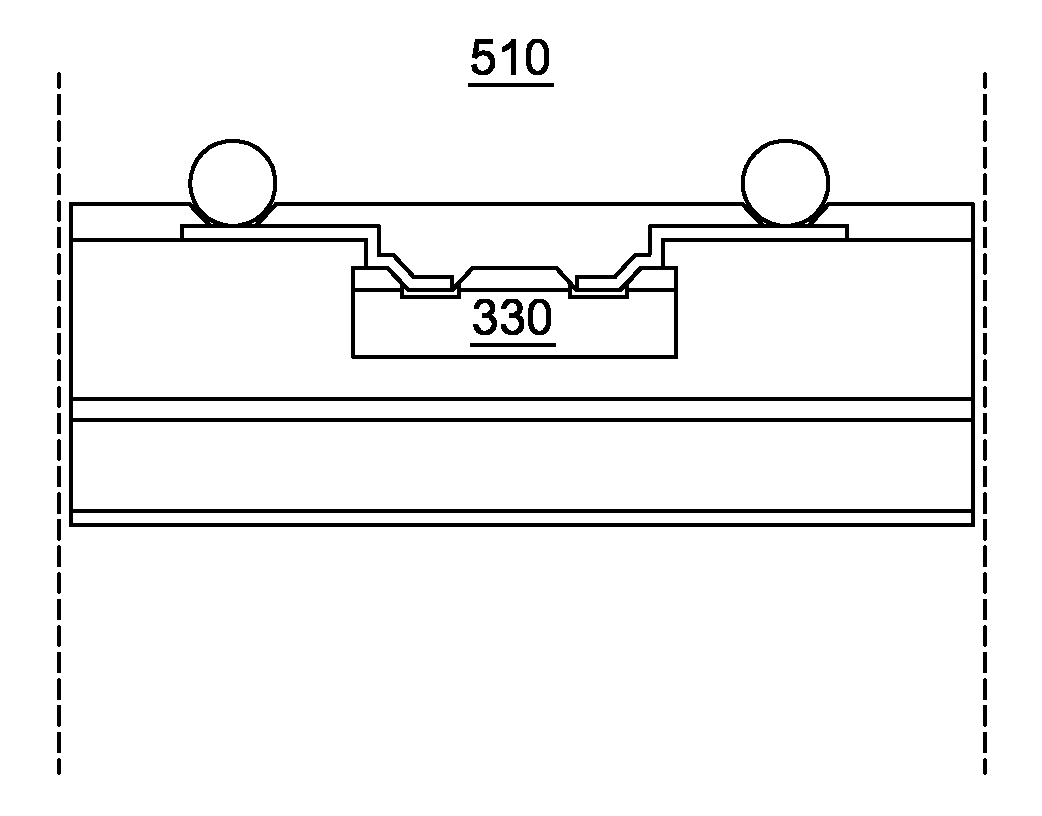
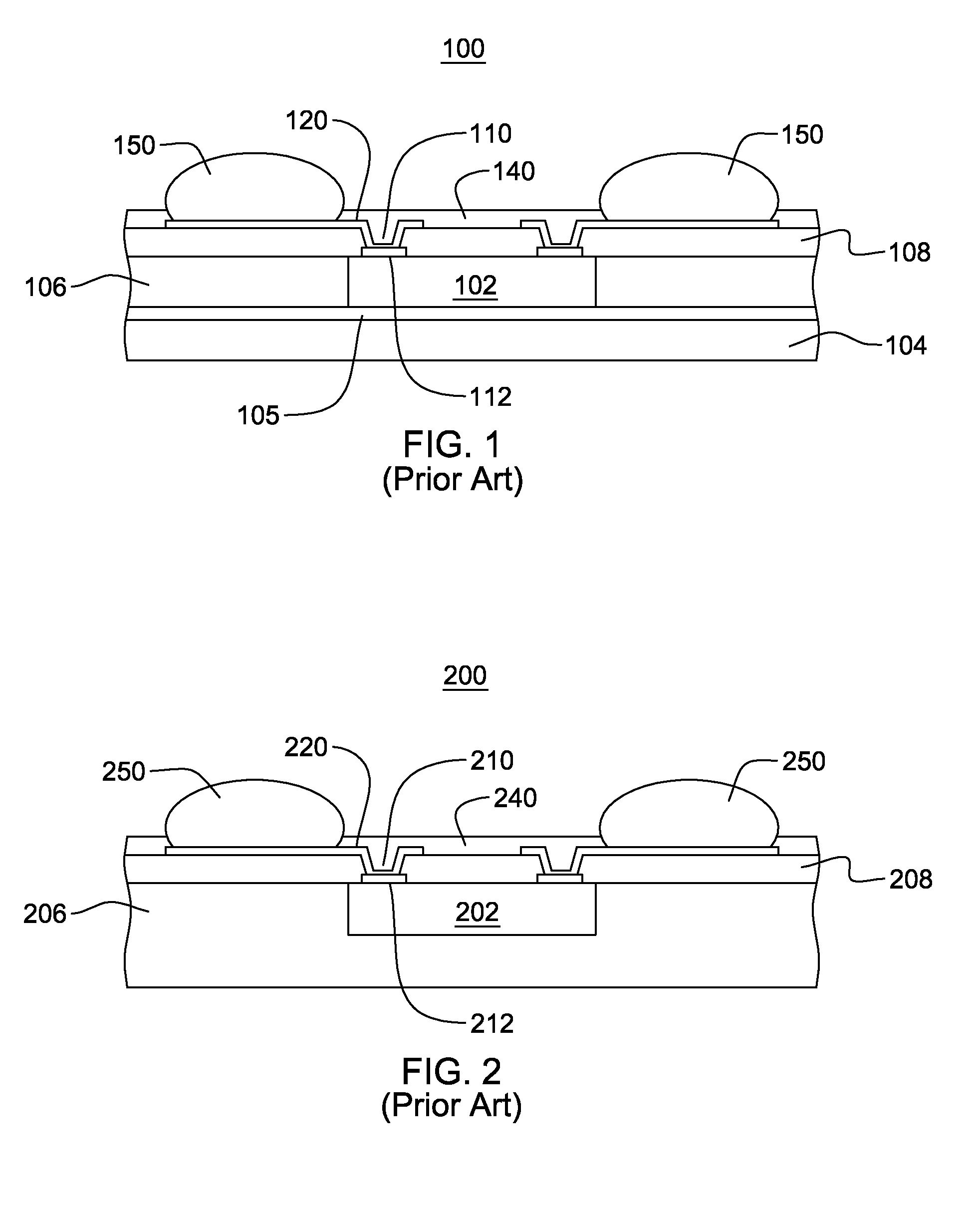
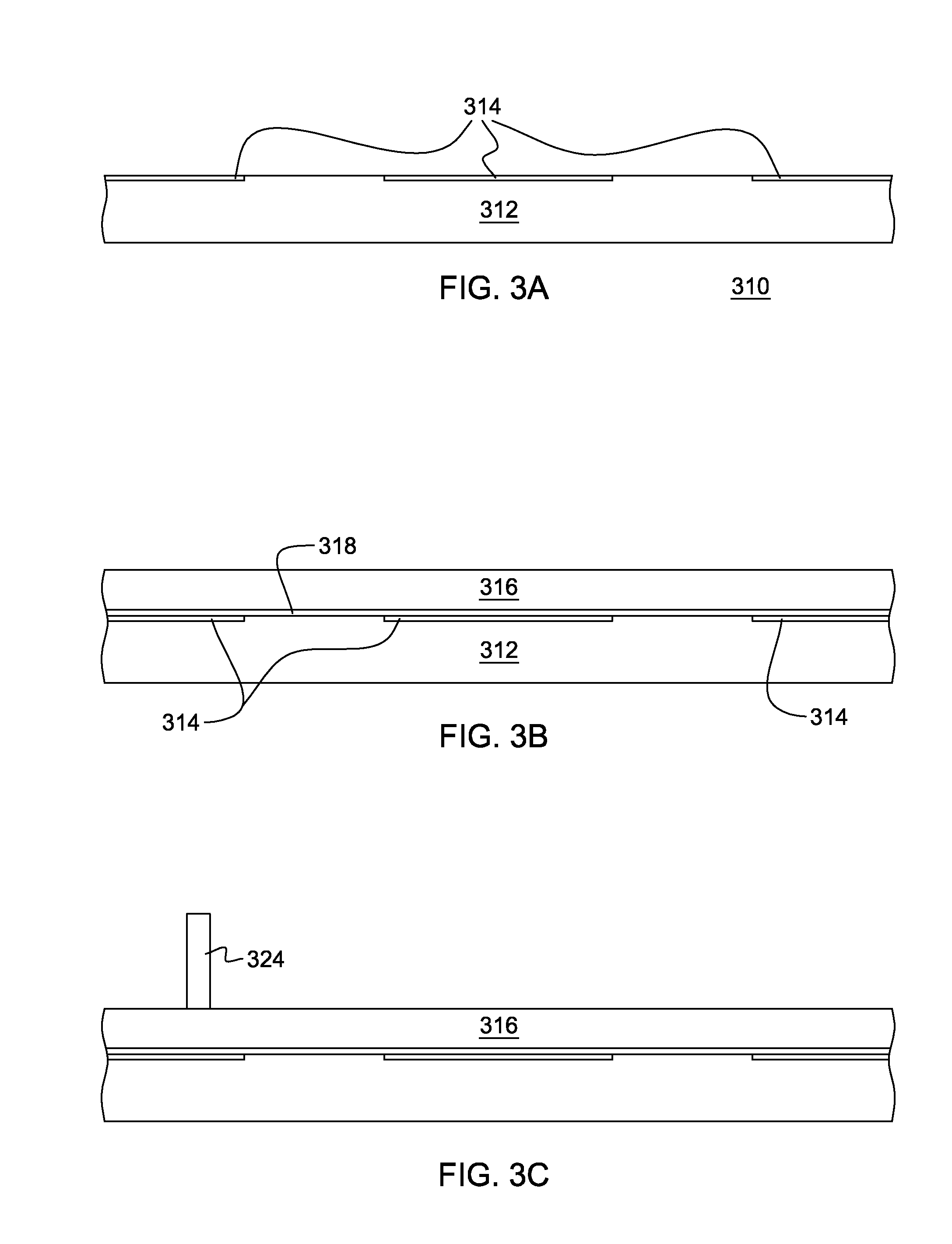
[0038]Generally stated, provided herein are numerous enhancements to multichip modules, and in particular, to chips-first multichip modules. Advantageously, described herein are structures and fabrication methods of a chips-first electronic module, wherein a first level metallization is applied directly to the front surface of the chips-first layer, without first applying a dielectric layer over the chips-first layer. Further, provided herein are structures and methods of fabrication which provide a chips-first electronic module with a fan-out metallization, where lithography steps are minimized, and only one lithography step is used for the fan-out metallization. In another aspect, structures and methods of fabricating a multi-layer, chips-first electronic module are described below, wherein a first level metallization is applied and patterned before a first level dielectric layer is applied to the chips-first structure. The electronic modules and methods of fabrication described h...


PUM

PropertyMeasurementUnit
Structureaaaaaaaaaa
Heightaaaaaaaaaa
Elongationaaaaaaaaaa

Abstract

Electronic modules and methods of fabrication are provided implementing a first metallization level directly on a chips-first chip layer. The chips-first layer includes chips, each with a pad mask over an upper surface and openings to expose chip contact pads. Structural dielectric material surrounds and physically contacts the side surfaces of the chips, and has an upper surface which is parallel to an upper surface of the chips. A metallization layer is disposed over the front surface of the chips-first layer, residing at least partially on the pad masks of the chips, and extending over one or more edges of the chips. Together, the pad masks of the chips, and the structural dielectric material electrically isolate the metallization layer from the edges of the chips, and from one or more electrical structures of the chips in the chips-first layer.

Description

CROSS-REFERENCE TO RELATED APPLICATIONS [0001]This application claims priority from U.S. Provisional patent application Ser. No. 60 / 945,988, filed Jun. 25, 2007, entitled “Integrated Structures and Fabrication Methods Thereof Implementing a Cell Phone or Other Electronic System”, by Eichelberger et al., the entirety of which is hereby incorporated by reference.TECHNICAL FIELD [0002]This invention relates in general to circuit structures and methods of fabrication thereof, and more particularly, to integrated structures and methods of fabrication thereof implementing a first level metallization directly on a chips-first chip layer.BACKGROUND OF THE INVENTION [0003]The conventional approach to electronic packaging and interconnect has been to package individual integrated circuit (IC) chips into a single package and to attach these packages to a printed circuit board to provide interconnect between the individual IC chips. In recent years, this approach has met with problems of speed...

Claims


Application Information

Patent Timeline
IPC IPC(8): H01L23/48H01L21/56
CPCH01L21/6835Y10T29/49147H01L23/3128H01L23/5389H01L23/552H01L24/18H01L25/0652H01L2221/68345H01L2224/04105H01L2224/16H01L2224/20H01L2224/211H01L2224/24137H01L2924/01011H01L2924/01013H01L2924/01015H01L2924/01018H01L2924/01027H01L2924/01029H01L2924/01032H01L2924/01049H01L2924/01074H01L2924/01077H01L2924/01078H01L2924/01082H01L2924/14H01L2924/15311H01L2924/15331H01L2924/19041H01L2924/19042H01L2924/19043H01L2924/30105H01L2924/30107H01L2924/3025H05K1/0206H05K1/0218H05K1/185H05K3/4644H05K2201/09563H05K2201/096H05K2201/10371H05K2201/10674H05K2203/0733H01L2924/01006H01L2924/01033H01L2924/3511H05K3/30H01L2924/10253H01L23/29Y10T29/49121H01L24/19H01L24/96H01L2224/12105H01L2225/1035H01L2225/1058H01L2224/0401Y10T29/49155Y10T29/49124Y10T29/4913Y10T29/49144H01L2924/00H01L2924/181H01L2924/12042H01L2223/6677H01L2224/2518H01L21/568H01L24/82H01L2224/16235H01L2224/16227H01L2224/96
Inventor KOHL, JAMES E.EICHELBERGER, CHARLES W.
Owner EPIC TECH INC
Why Eureka
Try Eureka