High voltage ESD protection featuring pnp bipolar junction transistor

a bipolar junction transistor and high-voltage technology, applied in the direction of transistors, electrical devices, arrangements responsive to excess voltage, etc., can solve the problems of esd protection schemes, device malfunction and/or destruction of esd protection circuits, and undesirable npn bjt-based esd protection, so as to reduce device area and leakage current, reduce the risk of latching, and high holding voltage

Inactive Publication Date: 2008-12-25
TEXAS INSTR INC
View PDF10 Cites 49 Cited by
  • Summary
  • Abstract
  • Description
  • Claims
  • Application Information

AI Technical Summary

Benefits of technology

[0019]Thus a high voltage ESD protection circuit is disclosed for protecting a semiconductor device, having a re

Problems solved by technology

This characteristic renders npn BJT-based ESD protection approaches undesirable, as this low holding voltage creates a potential risk of latch-up.
That is, the device may remain in a conducting or shorted state under powered-up normal operating conditions, which can result in a device malfunction and/or the destruction of the ESD protection circuit.
Consequently, ESD protection schemes, where the primary device is an npn bipolar transistor, may not be suitable for the prote

Method used


Image

  • High voltage ESD protection featuring pnp bipolar junction transistor
  • High voltage ESD protection featuring pnp bipolar junction transistor
  • High voltage ESD protection featuring pnp bipolar junction transistor

Examples


Embodiment Construction

[0028]The present invention will now be described with respect to the accompanying drawings in which like numbered elements represent like parts. The figures provided here and the accompanying description of the figures are merely provided for illustrative purposes. One of ordinary skill in the art should realize, based on the instant description, other implementations and methods for fabricating the devices and structures illustrated in the figures and in the following description.

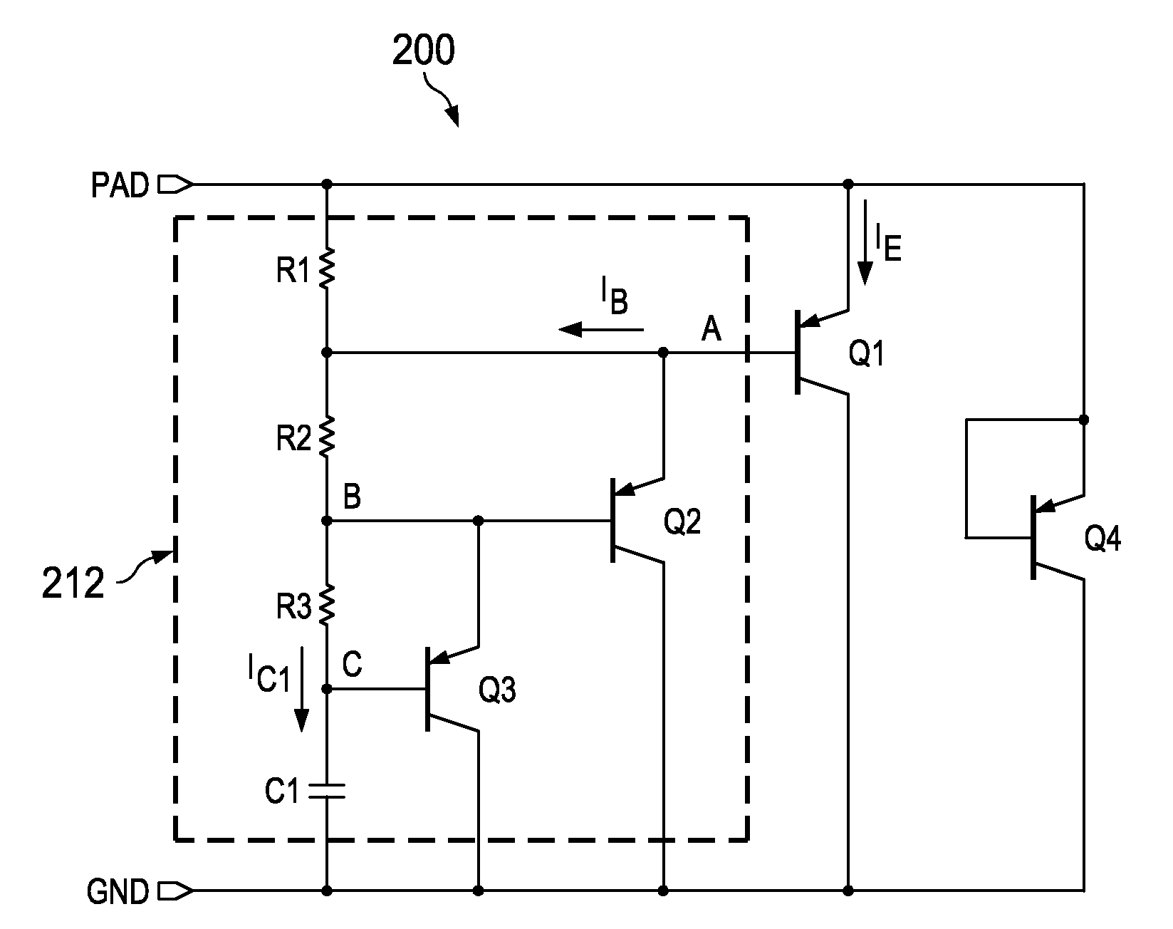
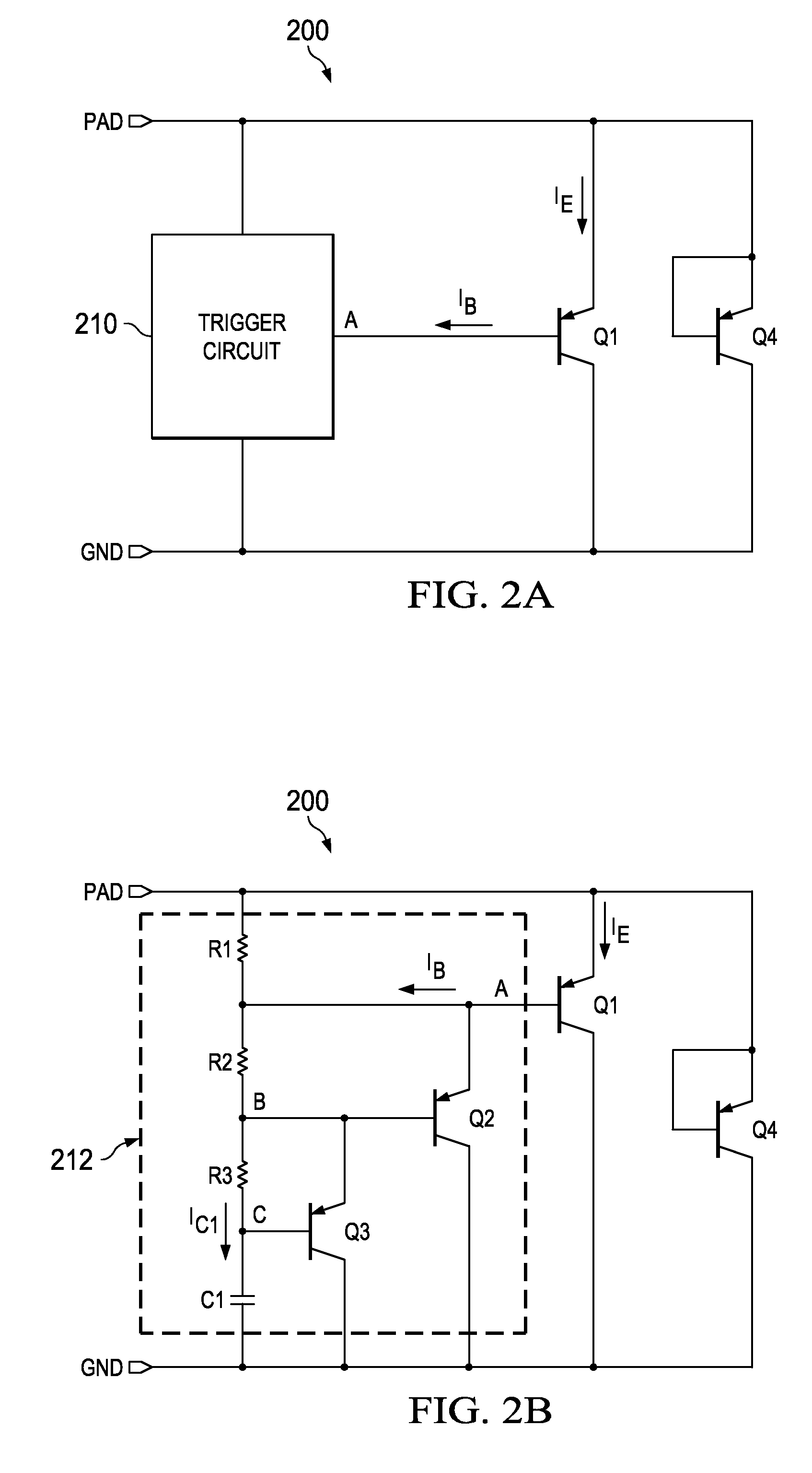
[0029]In the present invention, the primary device used for ESD protection is a pnp transistor. Holding voltage, the main device characteristic prohibiting the use of an npn transistor for ESD protection, can be considerably higher in a pnp transistor, and may actually exceed the maximum operating voltage of the device pin (terminal) to be protected. In that case, the pnp transistor could be used for ESD protection.

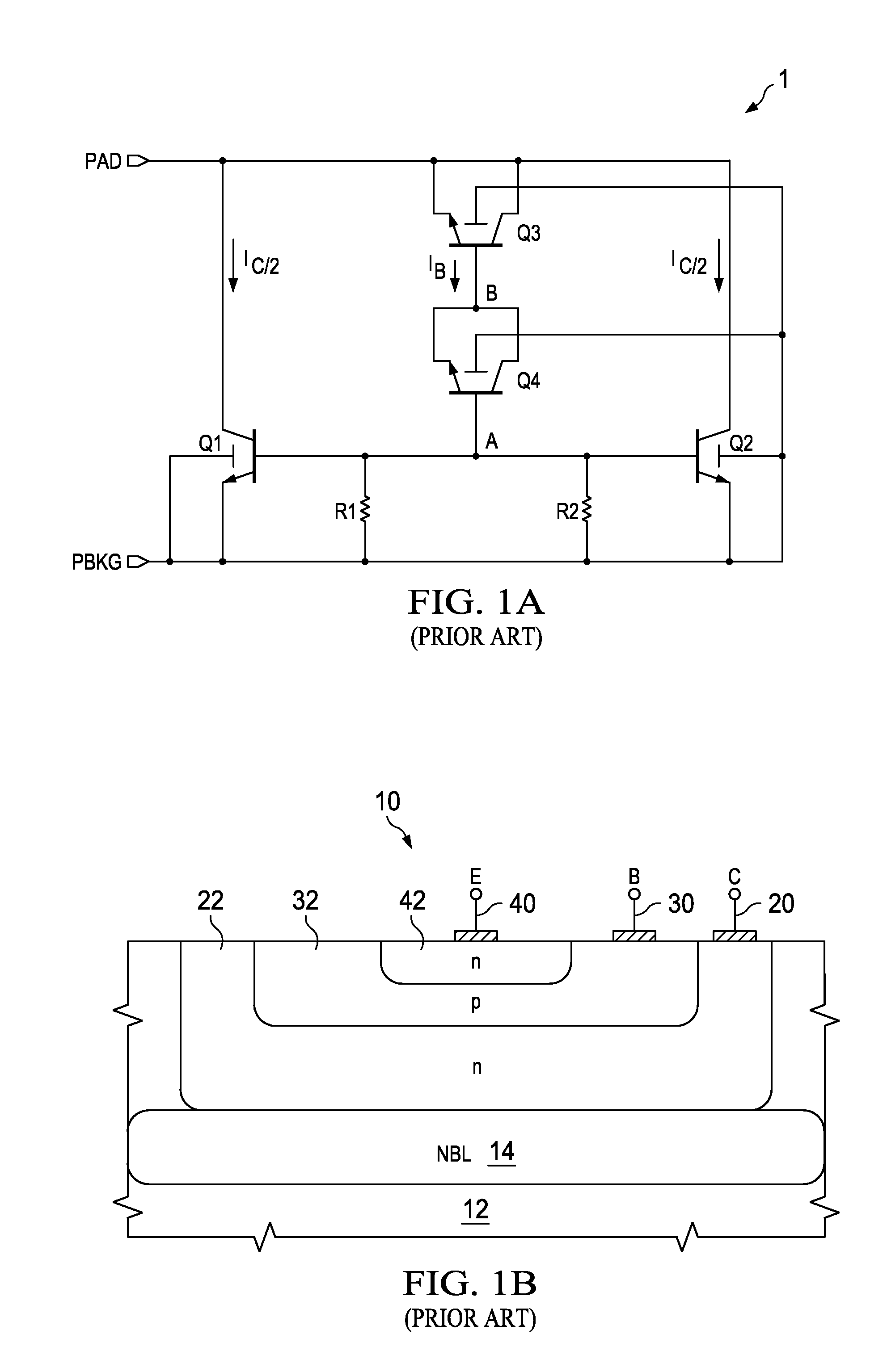
[0030]In a conventional homo-junction bipolar transistor (HBT) technology, the main drawbac...


PUM


Abstract

A protection circuit is disclosed that protects a semiconductor device from damage due to an electrostatic discharge. One such protection circuit comprises a vertical pnp hetero-junction bipolar transistor (HBT) connected between terminals such as supply terminals of the device, configured to conduct during an electrostatic discharge. The protection circuit also comprises a trigger circuit, such as a transient activated RC circuit connected between the terminals to detect the electrostatic discharge and control the transistor based on the detected electrostatic discharge. A Darlington transistor pair in the trigger circuit can be used to multiply the effective capacitance and HBT drive current. The HBT transistor absorbs energy from the electrostatic discharge and clamps the over-voltage across the terminals. The protection circuit may also be used across other I/O terminals of the device.

Description

FIELD OF THE INVENTION[0001]The present invention relates generally to semiconductor device fabrication, and more particularly, to an improved high voltage electrostatic discharge (ESD) protection circuit implemented as a transient activated, hetero-junction bipolar transistor (HBT) having reduced device area, a higher holding voltage, and reduced leakage current.BACKGROUND OF THE INVENTION[0002]A variety of electronic devices are sensitive to electrostatic discharge (ESD), whether the device is powered up and active, remains without power, or during handling of the device prior to assembly.[0003]The npn bipolar junction transistor (BJT), which is typically the device of choice for protection against ESD in BJT process technologies, suffers from low holding voltages (defined as the voltage at which a device goes into and remains in a low-impedance, conducting state; typically 5-10 V in an npn BJT) compared to the maximum operating voltage in high-voltage (typically larger than 10 V)...

Claims


Application Information

Patent Timeline
IPC IPC(8): H02H9/04H02H9/00
CPCH01L27/0259
Inventor OGUZMAN, ISMAIL HAKKIKUNZ, JR., JOHN ERIC
Owner TEXAS INSTR INC
Why Eureka
Try Eureka