Semiconductor device and method of forming the same

a technology of semiconductors and electrodes, applied in the direction of semiconductor devices, basic electric elements, electrical equipment, etc., can solve the problems of complex and troublesome etching to form the second gate electrode, and does not meet the demand of simplicity pursued by the industry, and achieves simple and easy process, simple and easy approach

Active Publication Date: 2008-12-25
UNITED MICROELECTRONICS CORP
View PDF22 Cites 33 Cited by
  • Summary
  • Abstract
  • Description
  • Claims
  • Application Information

AI Technical Summary

Benefits of technology

[0016]In the method of the present invention, only the lower electrode layer is selectively formed. The following silicon layer may entirely cover the lower electrode layer. In the method of the present invention, it is neither required to selectively etch the lower electrode layer nor to planarize the separately formed lower electrode layer and the silicon layer to the same surface, rather to primarily form a silicide layer made from the silicon layer. Obviously many complicated steps are omitted and this is a simple and easy approach. The advantages of the present invention reside in that the threshold voltages of each gate structure are determined by ingeniously taking the advantages of the difference of the work function between the silicide layer formed by the silicon layer and a metal and the lower electrode layer. Preferably, of the silicide layer and the lower electrode layer respectively in the two separate gate structures, one has the work function higher than the substrate's and the other one has a lower one. This is a simple and easy way to form the PMOS and the NMOS with different threshold voltages and to meet the demand of a more simplified process.

Problems solved by technology

It is clear that the concept of forming the first gate electrode material layer first and followed by the etching to form the second gate electrode is both complex and troublesome and does not meet the demand of simplicity pursued by the industry.

Method used


Image

  • Semiconductor device and method of forming the same
  • Semiconductor device and method of forming the same
  • Semiconductor device and method of forming the same

Examples


Embodiment Construction

[0020]The present invention first provides a semiconductor device which includes a PMOS and an NMOS. In one of which, one conductive material stacks on another one on the gate dielectric of the substrate to form a composite gate electrode and the other has only one conductive material to form a single electrode. Preferably, of the two conductive materials, one has the work function higher than the substrate's and the other one has a lower one to provide the different threshold voltages required by the PMOS and the NMOS.

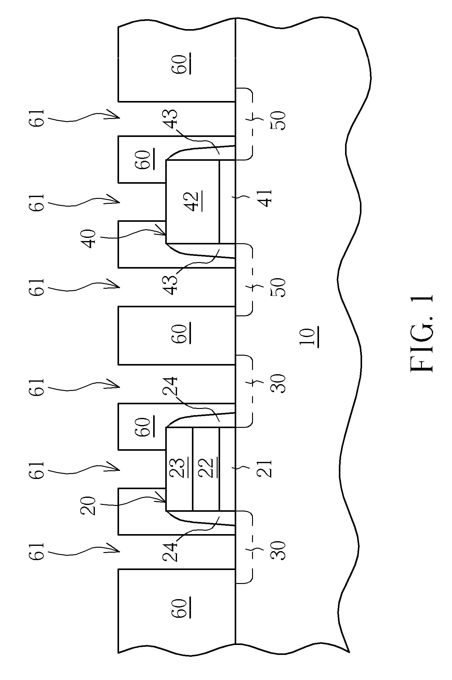
[0021]FIG. 1 illustrates a preferred embodiment of the semiconductor device of the present invention. Please refer to FIG. 1, the semiconductor device 1 of the present invention includes the substrate 10, the first gate structure 20, the first source / drain 30, the second gate structure 40, the second source / drain 50 and the interlayer dielectric 60 covering the substrate 10, the first gate structure 20, the first source / drain 30, the second gate structure 40 and the s...


PUM


Abstract

A semiconductor device includes a first gate structure including a gate dielectric layer directly contacting the substrate, a bottom electrode on the gate dielectric layer and a top electrode on the bottom electrode, and a second gate structure including a gate dielectric layer directly contacting the substrate and a gate electrode on the gate dielectric layer.

Description

CROSS REFERENCE TO RELATED APPLICATIONS[0001]This patent application is a divisional application of and claims priority to U.S. patent application Ser. No. 11 / 743,650, filed on May 2, 2007, and entitled “SEMICONDUCTOR DEVICE AND METHOD OF FORMING THE SAME,” the entire contents of which are incorporated herein by referenceBACKGROUND OF THE INVENTION[0002]1. Field of the Invention[0003]The present invention relates to a semiconductor device and the method for forming the same. More particularly, the present invention relates to a semiconductor device with two different MOS structures.[0004]2. Description of the Prior Art[0005]Metal-oxide-semiconductor field-effect transistor, MOSFET for short, is a widely used field-effect transistor. According to the polarity of its channel, the MOSFET is divided into the P-type and the N-Type, i.e. PMOS and NMOS.[0006]Functionally speaking, PMOS and NMOS each has different threshold voltages, which are determined by the difference of the work functi...

Claims


Application Information

Patent Timeline
Patent Type & Authority Applications(United States)
IPC IPC(8): H01L21/8238
CPCH01L21/823835H01L21/823842H01L21/823871H01L29/4966H01L29/665H01L29/7843
Inventor LIN, CHIEN-TINGCHENG, LI-WEIHSU, CHE-HUAHUANG, YAO-TSUNGMA, GUANG-HWA
Owner UNITED MICROELECTRONICS CORP
Why Eureka
Try Eureka