Organic Thin Film Transistor and Manufacturing Process the Same

Inactive Publication Date: 2009-01-01
NEC CORP
View PDF0 Cites 11 Cited by
  • Summary
  • Abstract
  • Description
  • Claims
  • Application Information

AI Technical Summary

Benefits of technology

[0059]The present invention can, conveniently and at low cost, provide a vertical organic thin film transistor exhibiting a high

Problems solved by technology

However, in this technique, it is difficult to prepare a polymer film comprising a microphase separation structure suitable for the process and this technique requires too many steps to be an inexpensive process.
When a gate electrode is etched over an organic semiconductor layer, the organic semiconductor layer is inevitably damaged, leading to difficulty in stably preparing an element exhibiting good

Method used


Image

  • Organic Thin Film Transistor and Manufacturing Process the Same
  • Organic Thin Film Transistor and Manufacturing Process the Same
  • Organic Thin Film Transistor and Manufacturing Process the Same

Examples


embodiment 1

(1) EMBODIMENT 1

[0071]There will be described a structure of an organic thin film transistor according to the first embodiment of the present invention.

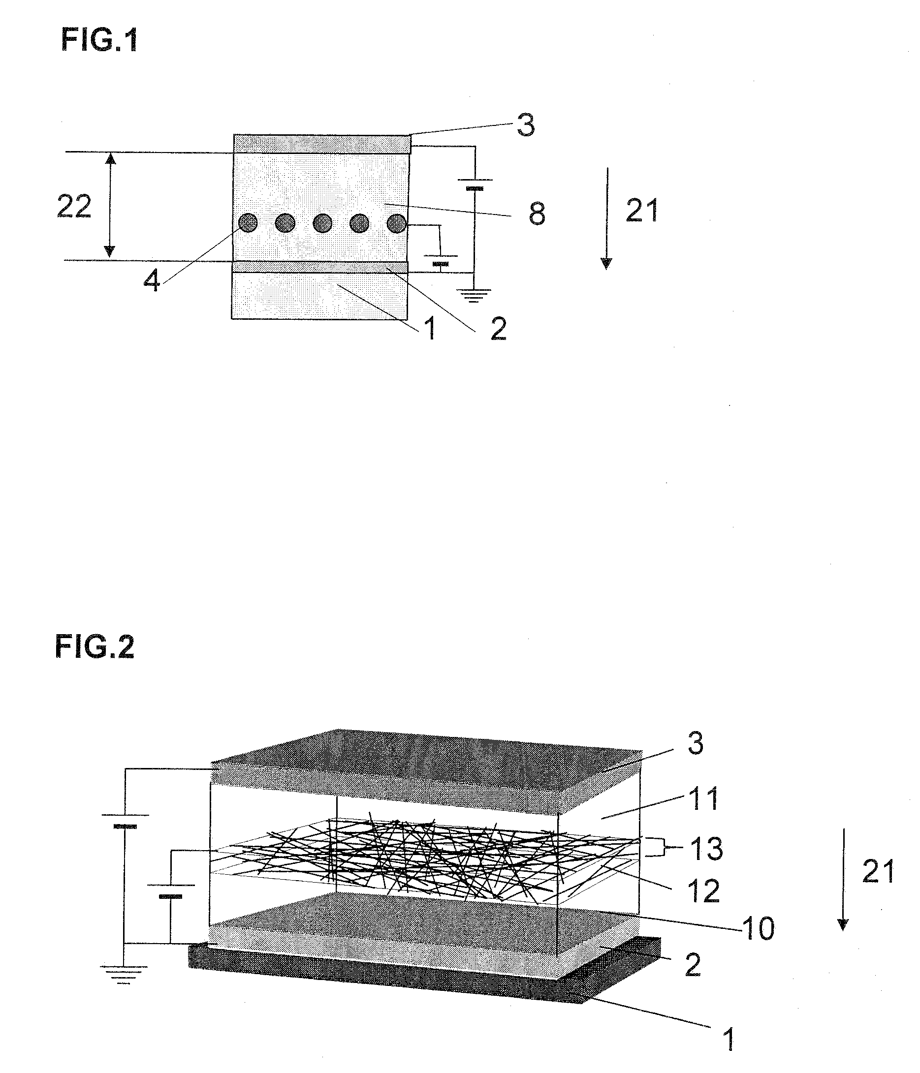
[0072]FIG. 2 shows an example of a structure of an organic thin film transistor comprising a gate electrode formed using a wire-shaped conductive material of the present invention. In this organic thin film transistor, a first organic semiconductor layer 10 is formed such that it contact a source electrode 2 formed over a supporting substrate 1. Furthermore, over the surface is disposed a gate electrode layer 13 having randomly positioned wire-shaped conductive materials 12. A second organic semiconductor layer 11 and a drain electrode 3 are further deposited in sequence over the gate electrode layer 13 to form an organic thin film transistor.

[0073]FIG. 8(a) shows a view of this gate electrode layer from above. FIG. 8b is an enlarged view of the region surrounded by a dot line of a gate electrode layer of FIG. 8(a). Individual wire-s...

embodiment 2

(2) EMBODIMENT 2

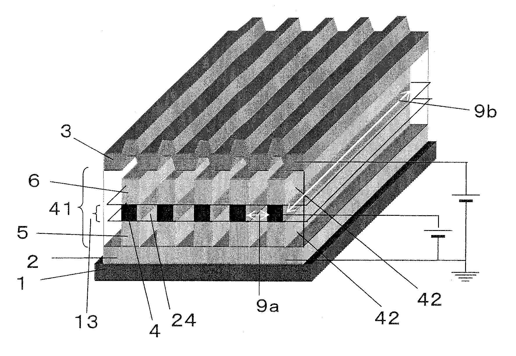
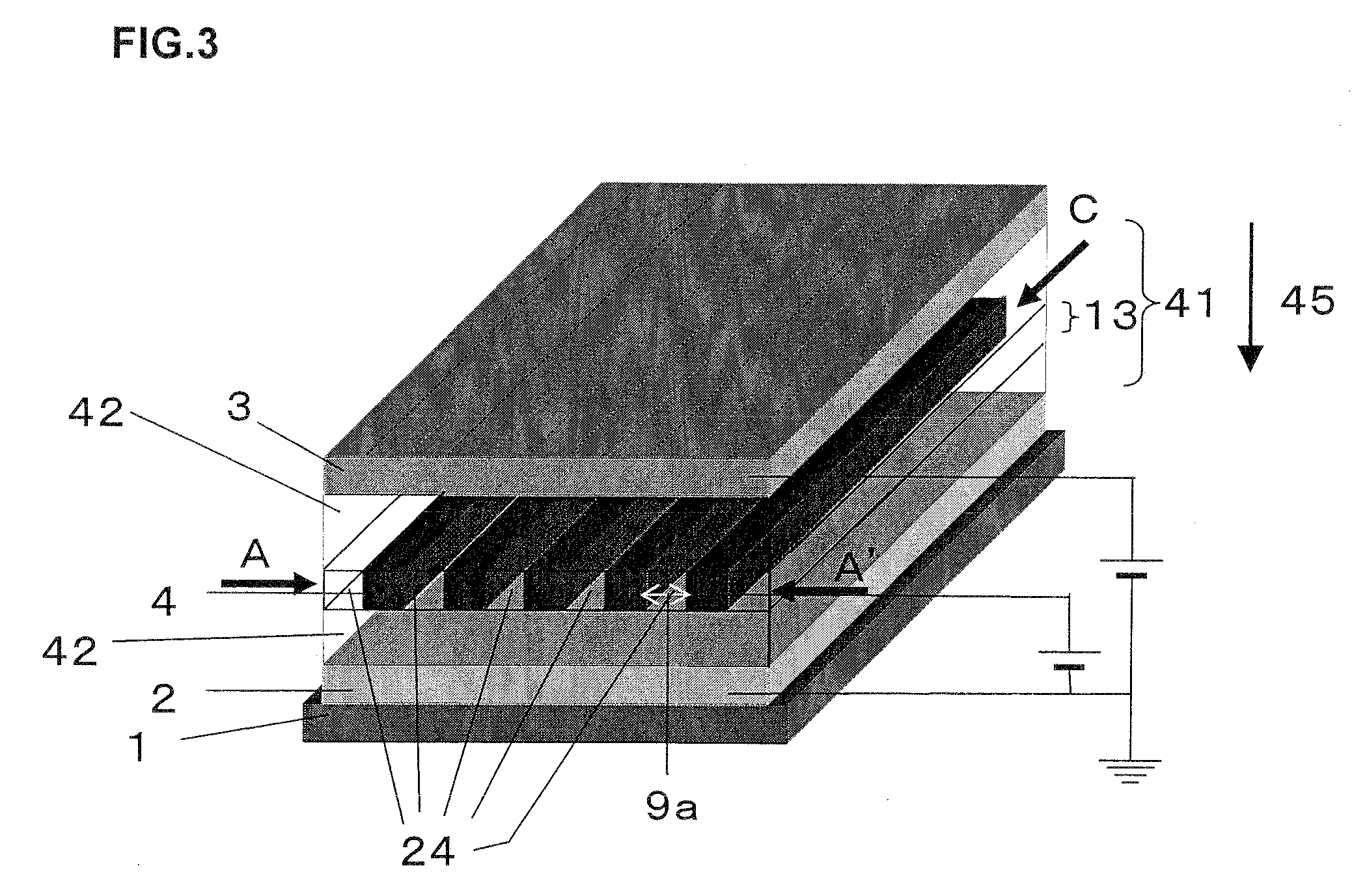
[0088]FIG. 3 shows an example of a structure of an organic thin film transistor according to the second embodiment of the present invention. In this organic thin film transistor, a source electrode 2 and a drain electrode 3 facing the source electrode 2 are formed on a supporting substrate 1 and an intermediate layer 41 is formed between a source electrode 2 and a drain electrode 3. This intermediate layer 41 comprises a gate electrode layer 13 formed such that it does not contact the source electrode 2 or the drain electrode 3, and an intermediate semiconductor portion 42 composed of an organic semiconductor material at least in part of the region between the gate electrode layer 13 and the source electrode 2 and at least in part of the region between the gate electrode layer 13 and the drain electrode 3. In the organic thin film transistor shown in FIG. 3, all the region between the gate electrode layer 13 and the source / drain electrode is the intermediate semicond...

embodiment 3

(3) EMBODIMENT 3

[0099]FIG. 5 shows an example of a structure of an organic thin film transistor according to the third embodiment of the present invention. This embodiment is a modification of Embodiment 2 and is different from Embodiment 2 in that an insulating film is formed covering a gate electrode surface in the second organic thin film transistor.

[0100]As in the second embodiment, this organic thin film transistor comprises a source electrode 2, an intermediate layer 41 and a drain electrode 3 over a supporting substrate 1, but is different in that the surface of a gate electrode in the gate electrode layer 13 present in the intermediate layer 41 is covered by an insulating film. There are no particular restrictions to a thickness of the insulating film or a covering pattern of the gate electrode surface as long as the effects of the present invention are achieved.

[0101]In an organic thin film transistor of the present invention, there is the semiconductor portion (B) between ...


PUM


Abstract

Described is a SIT type organic thin film transistor in which gate electrodes are formed as a conductive layer where a plurality of wire-shaped conductive materials are arranged in such a manner that a distance to the nearest wire is 100 nm or less at any point in the space between the wires or a semiconductor portion (B) between the gate electrodes has a rectangular cross section formed by a length of shorter sides in the range of 20 nm to 200 nm and a length of longer side 2 μm or more. This provides an organic thin film transistor which can be fabricated easily at a low temperature, at a low cost, and with high-speed drive ability, a high ON/OFF ratio, and a high controllability.

Description

TECHNICAL FIELD[0001]The present invention relates to an organic thin film transistor comprising an organic semiconductor material as an active layer and a manufacturing process the same.BACKGROUND OF THE INVENTION[0002]Thin film transistors (TFTs) have been extensively used as a pixel switching element for a display unit such as a liquid-crystal display and an EL display. Recently, pixel array driver circuits have been increasingly formed on the same substrate by the use of TFTs. Such TFTs have been formed on a glass substrate using amorphous or polycrystal silicon. However, a CVD apparatus used for preparing such a silicon-based TFT is very expensive, leading to a problem of significant increase in a manufacturing cost associated with producing a larger-area display unit using TFTs.[0003]Furthermore, since a process for depositing amorphous or polycrystal silicon is conducted at an extremely high temperature, there are limits to materials which can be used as a substrate; specific...

Claims


Application Information

Patent Timeline
IPC IPC(8): H01L51/00H01L51/40
CPCB82Y10/00H01L51/055H01L51/0048H10K85/221H10K10/481
Inventor TOGUCHI, SATORUENDOH, HIROYUKI
Owner NEC CORP
Why Eureka
Try Eureka