Method and apparatus for extracting properties of interconnect wires and dielectrics undergoing planarization process

a technology of dielectrics and interconnection wires, which is applied in the direction of basic electric elements, semiconductor/solid-state device testing/measurement, instruments, etc., can solve the problems of significant timing delay in circuits, non-uniformity of conductor wires and dielectric thicknesses, and product yield loss, so as to achieve fast and reliable, effective and efficient solutions

Inactive Publication Date: 2009-01-01
LIN WALLACE W
View PDF6 Cites 2 Cited by
  • Summary
  • Abstract
  • Description
  • Claims
  • Application Information

AI Technical Summary

Benefits of technology

[0007]The present invention for the first time presents an art of simultaneous extraction for the properties of the interconnect wires and the inter-wire dielectrics exposed to the IC planarization process. The art is achieved with a set of simple interconnect-wire structures by slightly varying (or perturbing), one at a time, one physical parameter in one structure while keeping the remaining physical parameters the same in remaining structures. Since the method is electrical based, it is extremely fast and reliable comparing with the physical measurements currently used for measuring the properties of the interconnect wires and the inter-wire dielectrics. The capability of handling a large amount of data in a short time scale makes this invented method particularly suitable for use in IC fabrication plants,
[0008]The method and apparatus presented in this invention, when used in collaboration with or embedded in other test structures that are well designed to cover a broad spectrum of interconnect wire layout features and scenarios, will provide an effective and efficient solution for characterizing and evaluating the impact of the IC planarization process on the interconnect wire and dielectric properties in circuit layouts on a full-chip level.

Problems solved by technology

Consequently, increasingly smaller, more compact and more delicate features of the interconnect wires are becoming essential to handle such formidable task in the design and manufacture of the ICs.
However, the smaller, more compact and more delicate interconnect wire features are beginning to interact with the IC manufacturing processes, causing product yield loss.
The interaction between the interconnect wire features and the planarization process of the interconnect conductor and dielectric layers such as, but not limited to, the chemical-mechanical polish (CMP) process, can cause non-uniformity of the conductor wire and dielectric thickness due to the dishing on the conductor wire surface and the erosion on the dielectric surface.
Such effect reduces thickness of the interconnect conductor and dielectric layers, thus increasing the conductor wire resistance and the dielectric capacitance which can cause significant timing delays in circuits.
Since there can be up to ten or more interconnect conductor and dielectric layers in the 65-nanometer technologies and beyond, the accumulated effect of the non-uniformity of the interconnect wire and dielectric thickness can be formidable after all interconnect conductor and dielectric layers receive the planarization process.
Technologies involved in such planarization process in the semiconductor industry to date has not yet arrived at a good solution in containing the aforementioned manufacture yield problem caused by the interaction between the fine features of the interconnect wires and the planarization process.
Physical characterization methods are generally accurate but time-consuming.
Moreover, the interconnect wire dishing and the inter-wire dielectric erosion have not yet been characterized directly and simultaneously by the electrical methods to date.

Method used


Image

  • Method and apparatus for extracting properties of interconnect wires and dielectrics undergoing planarization process
  • Method and apparatus for extracting properties of interconnect wires and dielectrics undergoing planarization process
  • Method and apparatus for extracting properties of interconnect wires and dielectrics undergoing planarization process

Examples


Embodiment Construction

[0012]In the following detailed description, reference is made to the accompanying drawings which form a part hereof wherein like numerals designate like parts throughout, and in which is shown by way of illustration specific embodiments in which the invention may be practiced. It is to be understood that other embodiments may be utilized and structural or logical changes may be made without departing from the scope of the present invention. Therefore, the following detailed description is not to be taken in a limiting sense, and the scope of the present invention is defined by the appended claims and their equivalents.

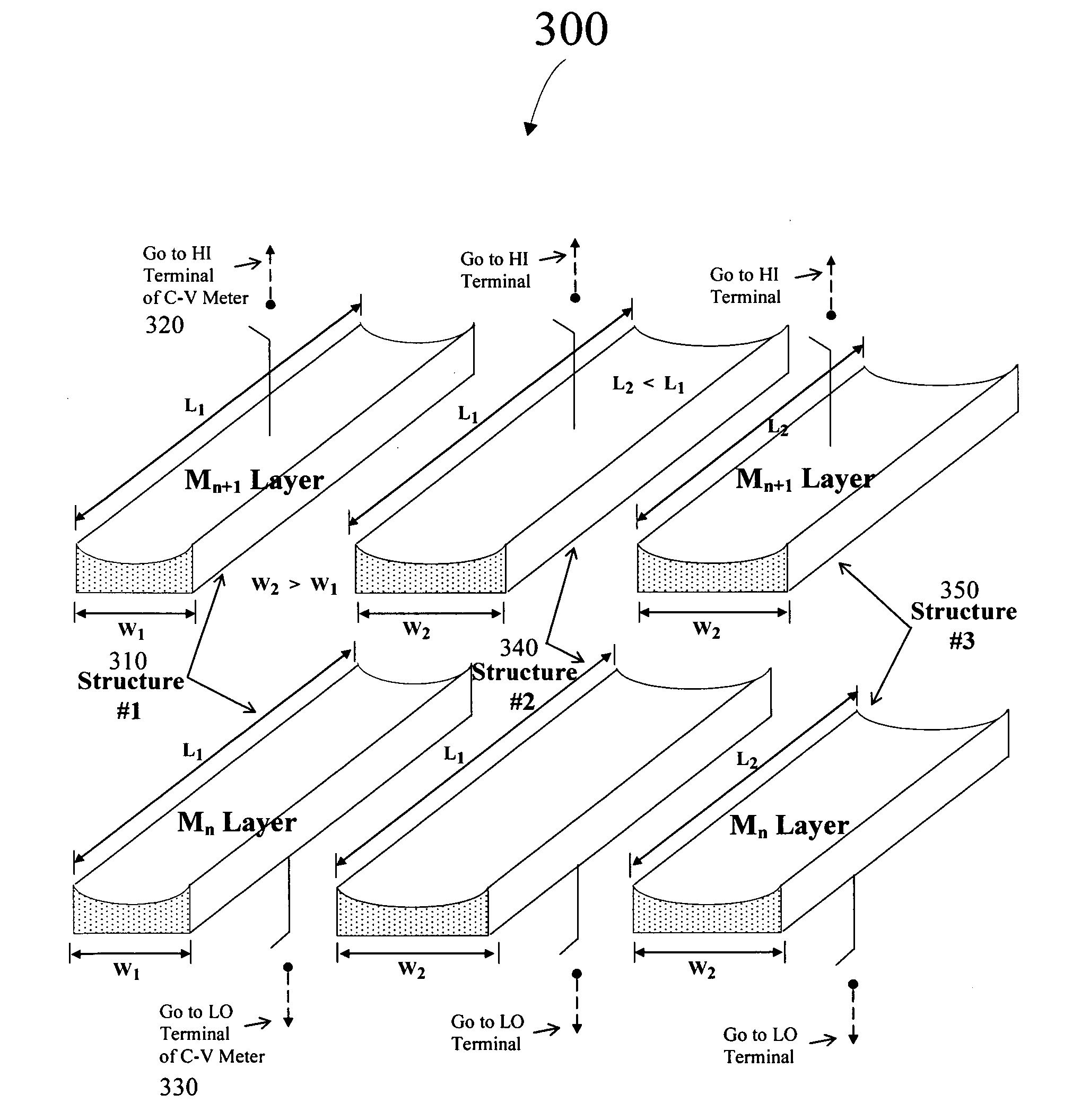
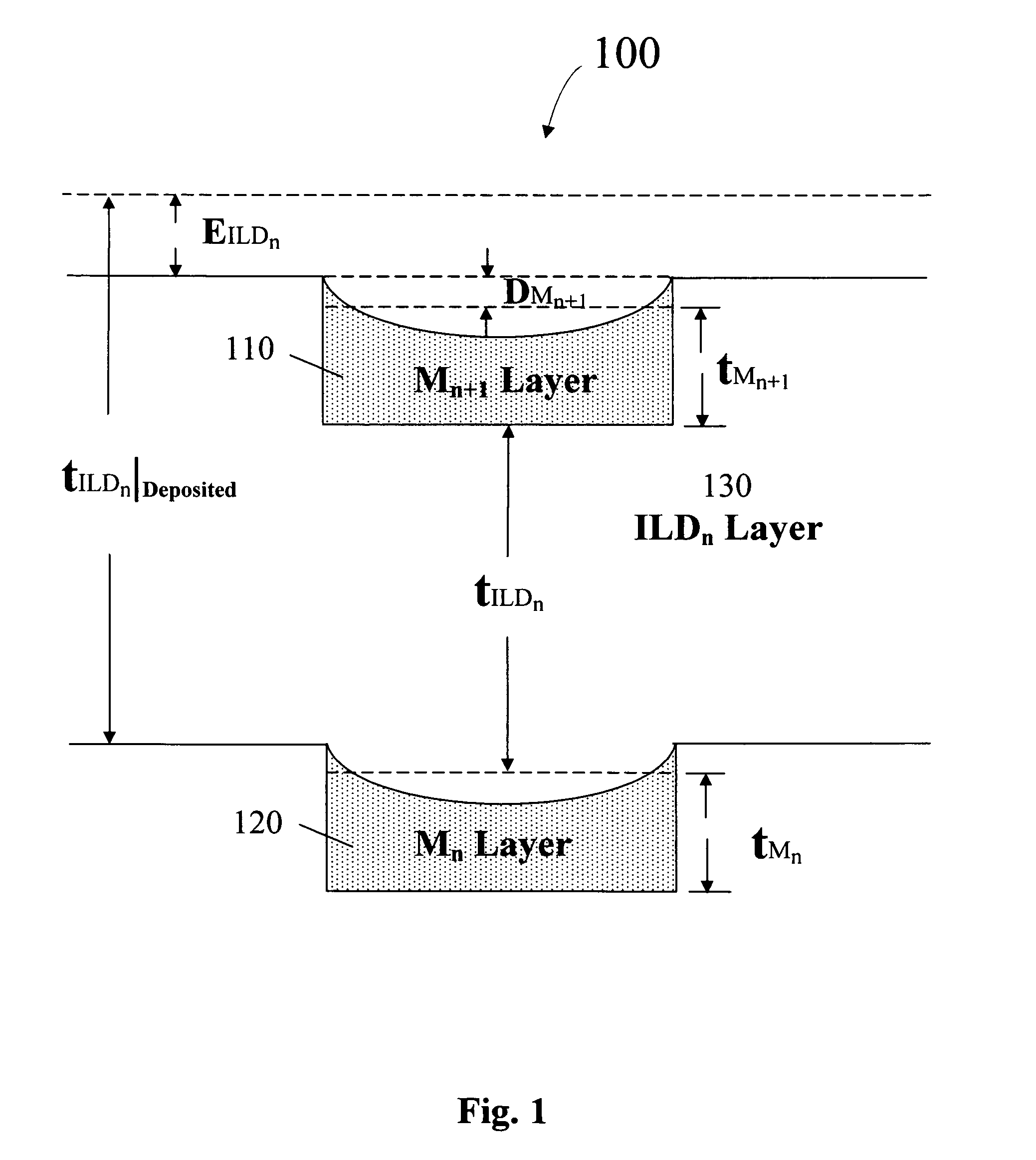
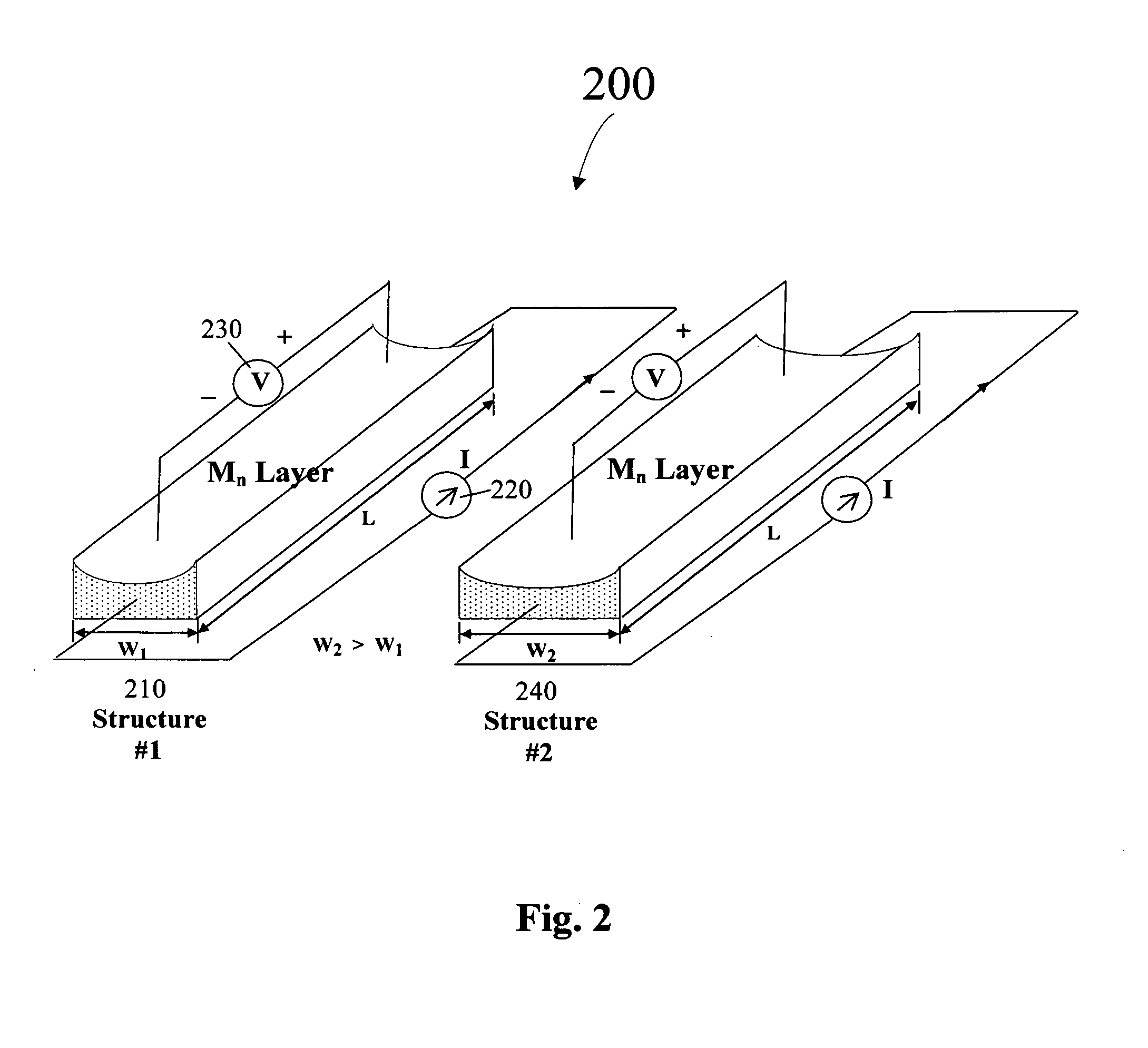
[0013]The Illustration 100 in FIG. 1 shows the cross sectional view of the interconnect wire layers of an IC layout after the planarization process. The concave shape of the metal wire is caused by the dishing effect from the planarization process. Given a total of n layers of the interconnect wires formed during an IC manufacture process, tMn denotes the metal thickn...


PUM


Abstract

The present invention provides a novel solution for simultaneously extracting the properties of the interconnect wires and the inter-wire dielectrics exposed to the IC planarization process.

Description

CROSS-REFERENCE TO RELATED APPLICATION[0001]This application claims priority of a provisional application Ser. No. 60 / 946,947, filed on Jun. 28, 2007.FIELD OF THE INVENTION[0002]The present invention relates to a method for simultaneously extracting the properties of the interconnect wires and the inter-wire dielectrics interacted with the planarization process during integrated-circuit manufacture.BACKGROUND OF THE INVENTION[0003]Trends in the design and manufacture of microelectronic dies, or integrated circuits (ICs) are toward increasing miniaturization, circuit density, robustness, operating speeds and switching rates, while reducing power consumption and defects in the ICs. ICs are made up of a tremendous number (e.g., millions to hundreds of millions) of devices (e.g., transistors, diodes, capacitors, etc.), with each component being made up of a number of delicate structures, manufactured through a number of process steps. As IC manufacture technology continues to evolve and...

Claims


Application Information

Patent Timeline
Patent Type & Authority Applications(United States)
IPC IPC(8): H01L23/58G01R31/12
CPCH01L22/32H01L2924/0002H01L2924/00
Inventor LIN, WALLACE W.
Owner LIN WALLACE W
Why Eureka
Try Eureka