Doped Diamond LED Devices and Associated Methods

a diamond led and led device technology, applied in the field of semiconductor/solid-state device manufacturing, semiconductor devices, electrical apparatus, etc., can solve the problems of increasing speed and reducing size of electronic circuits, various thermal problems, and difficulty in cooling such devices, so as to improve thermal properties and methods

Active Publication Date: 2009-01-01
SUNG CHIEN MIN
View PDF7 Cites 12 Cited by
  • Summary
  • Abstract
  • Description
  • Claims
  • Application Information

AI Technical Summary

Benefits of technology

[0007]Accordingly, the present invention provides semiconductor devices having improved thermal properties and methods for making such devices. In one aspect, for example, an LED device is provided having a conductive diamond layer, a SiC layer coupled to the diamond layer, a plurality of nitride semiconductor layers, at least one of which is coupled to the SiC layer, and an n-type electrode coupled to at least one of the plurality of nitride layers. Although numerous configurations for semiconductor layers are contemplated, in one aspect the plurality of semiconductor layers is arranged in series between the conductive diamond layer and the n-type electrode. Depending on the various techniques used to deposit a material, the crystal lattice of the SiC layer may be epitaxially coupled or matched to the crystal lattice of the conductive diamond layer. Additionally, the crystal lattice of the SiC layer may be epitaxially coupled or matched to the crystal lattice of at least one of the semiconductor layers.

Problems solved by technology

As electronic circuitry increases in speed and decreases in size, cooling of such devices becomes problematic.
As it builds, heat can cause various thermal problems associated with such electronic components.
Significant amounts of heat can affect the reliability of an electronic device, or even cause it to fail by, for example, causing burn out or shorting both within the electronic components themselves and across the surface of the printed circuit board.
Thus, the buildup of heat can ultimately affect the functional life of the electronic device.
This is particularly problematic for electronic components with high power and high current demands, as well as for the printed circuit boards that support them.
As increased speed and power consumption cause increasing heat buildup, such cooling devices generally must increase in size to be effective and may also require power to operate.
The demand for smaller electronic devices, however, not only precludes increasing the size of such cooling devices, but may also require a significant size decrease.

Method used


Image

  • Doped Diamond LED Devices and Associated Methods
  • Doped Diamond LED Devices and Associated Methods
  • Doped Diamond LED Devices and Associated Methods

Examples


example 1

[0074]A semiconductor substrate may be formed as follows:

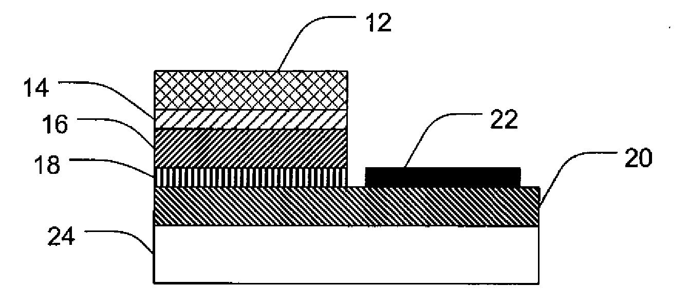
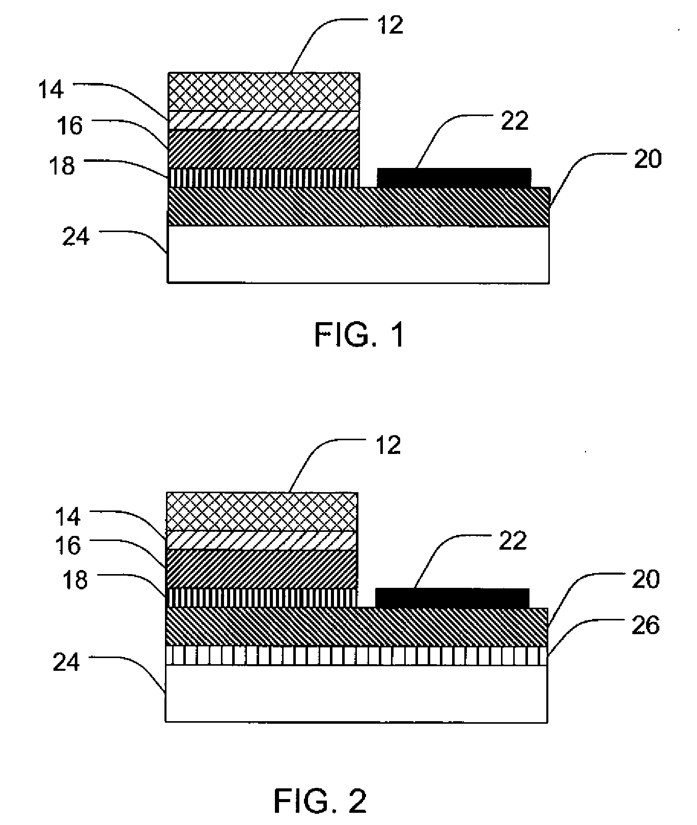
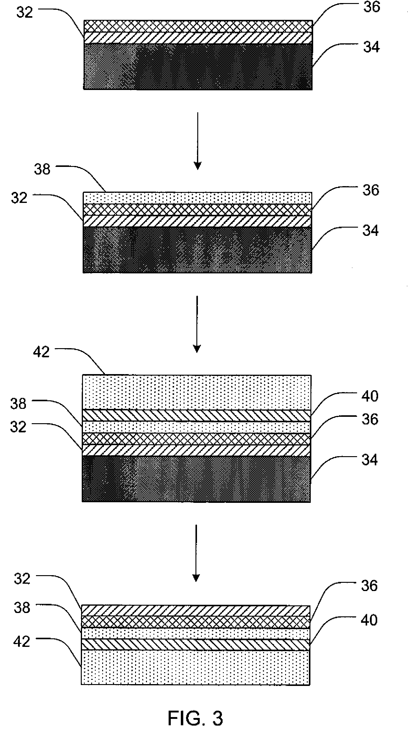
[0075]A single crystal Si wafer is obtained and cleaned by soaking in KOH and ultrasound cleaning with distilled water to remove any non-crystalline Si and foreign debris. A conformal amorphous carbon coating is applied to the cleaned surface of the Si wafer by exposing the wafer to CVD deposition conditions without an applied bias. Following carbonization of the surface, amorphous diamond is deposited for approximately 30 minutes at 800° in 1% CH4 and 99% H2. The amorphous carbon coating is then removed with H2 or F2 treatment for about 60 minutes, at 900°. Removal of the amorphous carbon coating exposes an epitaxial SiC layer that has formed in situ between the Si wafer and the amorphous carbon coating. The thickness of the SiC layer is approximately 10 nm.

[0076]A transparent diamond coating 10 microns thick is then deposited onto the SiC layer by CVD deposition of CH4 for approximately 10 hours. After 10 hours, the CH4 sour...

example 2

[0078]An LED device may be constructed as follows:

[0079]A semiconductor substrate is obtained as in Example 1. GaN semiconductor layers are deposited onto the exposed SiC layer by MOCVD with GaH3 and NH3 source materials.


PUM

PropertyMeasurementUnit
bond lengthaaaaaaaaaa
temperaturesaaaaaaaaaa
thicknessaaaaaaaaaa

Abstract

LED devices and methods for making such devices are provided. One such method may include forming epitaxially a substantially single crystal SiC layer on a substantially single crystal Si wafer, forming epitaxially a substantially single crystal diamond layer on the SiC layer, doping the diamond layer to form a conductive diamond layer, removing the Si wafer to expose the SiC layer opposite to the conductive diamond layer, forming epitaxially a plurality of semiconductor layers on the SiC layer such that at least one of the semiconductive layers contacts the SiC layer, and coupling an n-type electrode to at least one of the semiconductor layers such that the plurality of semiconductor layers is functionally located between the conductive diamond layer and the n-type electrode.

Description

PRIORITY DATA[0001]This application claims the benefit of U.S. Provisional Patent Application Ser. No. 60 / 932,803, filed on May 31, 2008, which is incorporated herein by reference.FIELD OF THE INVENTION[0002]The present invention relates generally to semiconductor devices and associated methods. Accordingly, the present invention involves the electrical and material science fields.BACKGROUND OF THE INVENTION[0003]In many developed countries, major portions of the populations consider electronic devices to be integral to their lives. Such increasing use and dependence has generated a demand for electronics devices that are smaller and faster. As electronic circuitry increases in speed and decreases in size, cooling of such devices becomes problematic.[0004]Electronic devices generally contain printed circuit boards having integrally connected electronic components that allow the overall functionality of the device. These electronic components, such as processors, transistors, resisto...

Claims


Application Information

Patent Timeline
Patent Type & Authority Applications(United States)
IPC IPC(8): H01L33/00H01L21/00H01L33/34H01L33/64
CPCH01L33/34H01L33/641Y10S438/931H01L33/32H01L33/0025
Inventor SUNG, CHIEN-MIN
Owner SUNG CHIEN MIN
Why Eureka
Try Eureka