Structure and method for wire bond integrity check on BGA substrates using indirect electrical interconnectivity pathway between wire bonds and ground

a technology of interconnection pathway and wire bond integrity, which is applied in the direction of semiconductor/solid-state device testing/measurement, soldering apparatus, auxilary welding devices, etc., can solve the problems of high density line/space pcb/substrat design with ball pads, circuit speed and complexity increase, and the necessity of packaging methods greatly affected

Inactive Publication Date: 2009-01-01
CYPRESS SEMICON CORP
View PDF0 Cites 23 Cited by
  • Summary
  • Abstract
  • Description
  • Claims
  • Application Information

AI Technical Summary

Problems solved by technology

As in every aspect of integrated circuit processing, packaging methods have of necessity been greatly affected as critical dimensions decrease and circuit speed and complexity increases.
A problem exists for the high density line / space PCB / substrate designs with ball pad OSP, which do not have a direct circuit connection on the top copper layer from the bond fingers to the tie bar and therefore to the grounded mold gate, whereas the layout of the bottom copper layer connects the ball pads to the bottom side tie bar.
(Verification of via quality has become necessary, since historically, use of poor drill bits for creating the via holes could cause uneven breaking of the resin, which could in turn result in incomplete copper plating and poor electrical connectivity.
As a result, the bond finger connected to that via hole would be improperly Ni—Au plated.)
However, not having the bond fingers connected to the top side tie bar prevents a closed circuit which would allow for the automatic wire bonding circuit integrity check.

Method used


Image

  • Structure and method for wire bond integrity check on BGA substrates using indirect electrical interconnectivity pathway between wire bonds and ground
  • Structure and method for wire bond integrity check on BGA substrates using indirect electrical interconnectivity pathway between wire bonds and ground
  • Structure and method for wire bond integrity check on BGA substrates using indirect electrical interconnectivity pathway between wire bonds and ground

Examples


Embodiment Construction

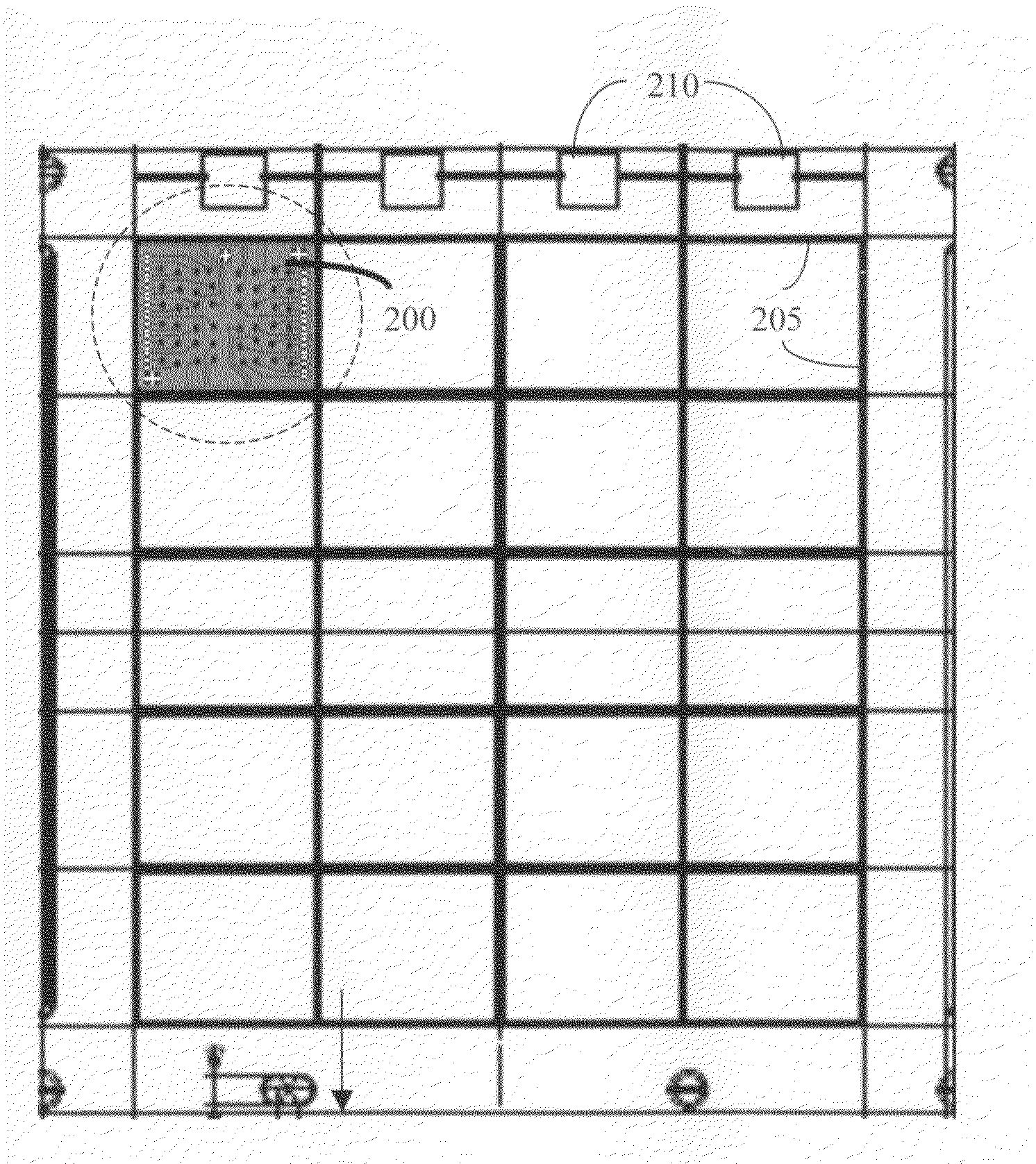
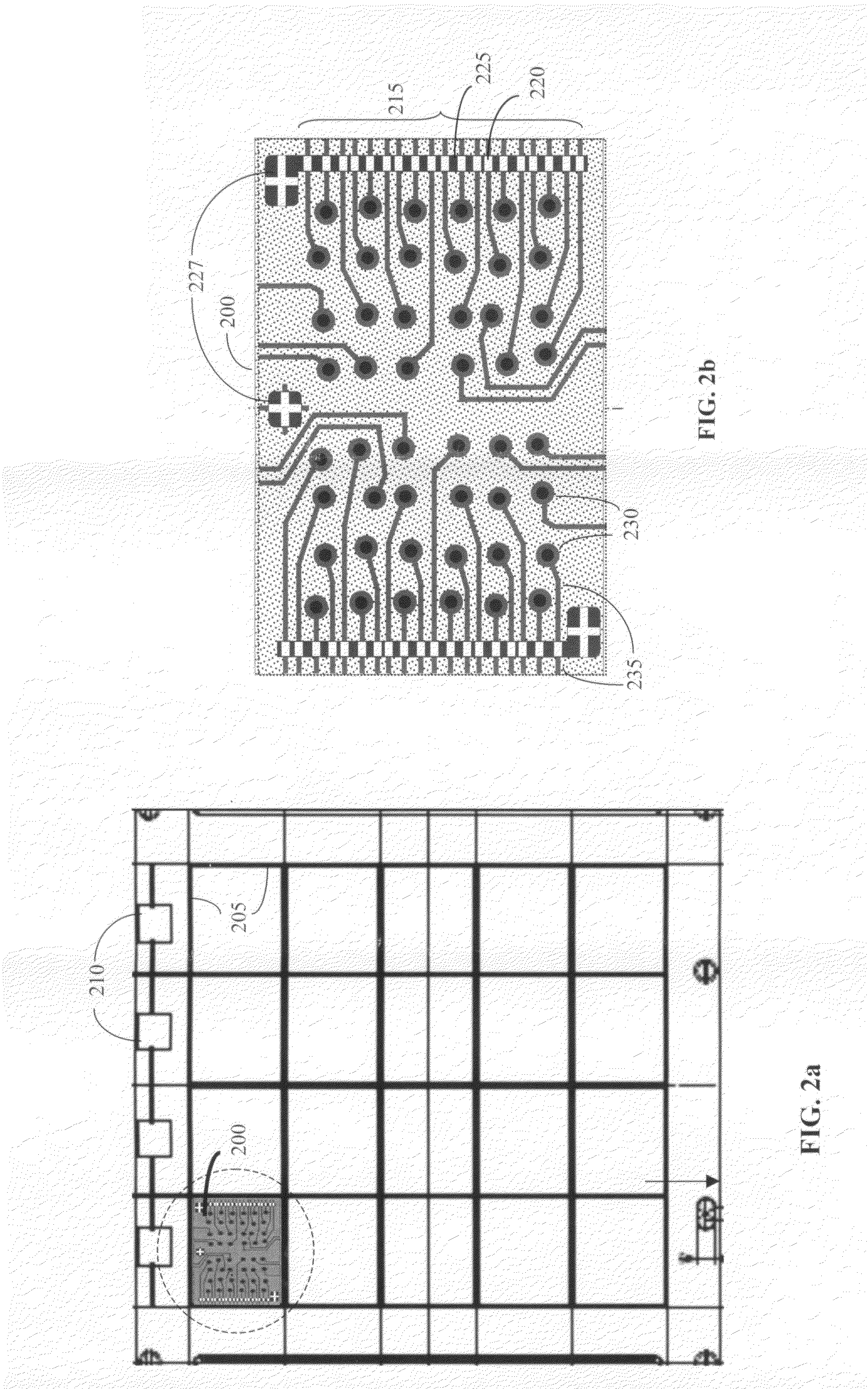
[0032]FIG. 2a shows a portion of a traditional PCB / substrate strip layout, from the top view. Regions 200 each comprise the substrate portion of a single BGA IC package body. Regions 200 are bordered by conducting Top Tie Bars 205. Mold gates 210 are connected to top tie bars 205, and are in a region outside BGA package body 200. When the packages are separated, also known as singulated, tie bars 205 are separated from substrate regions 200. As described in FIG. 1, the singulation occurs after the IC die is mounted on the substrate, wire bonds are made, the package is molded, and solder balls are attached. The singulated, molded package with IC mounted and bonded and solder balls attached is known as a “singulated unit”.

[0033]FIG. 2b shows a detailed region of FIG. 2a, showing a single portion 200 of a single BGA IC package body. Bond finger solder resist openings 215 expose conducting bond fingers 220, to which wire bonds to the IC are attached, and insulating regions 225. Fiducial...


PUM

PropertyMeasurementUnit
electrical integrityaaaaaaaaaa
electricalaaaaaaaaaa
electricallyaaaaaaaaaa

Abstract

An invention providing improvement in integrity testing of wire bonds between an IC die and a BGA substrate.The invention includes a BGA integrated circuit package comprising:1) a BGA substrate having conducting bond fingers and a grounded feature on a first side thereof; 2) an IC die electrically connected to the conducting bond fingers with wire bonds; the BGA substrate configured to be formed into a singulated unit with the IC die; wherein the BGA substrate does not have direct electrical connection on the first side thereof between the bond fingers and the grounded feature; 4) the BGA substrate including an indirect electrical connection pathway from each wire bond to the grounded feature that enables electrical integrity testing for the wire bonds; the indirect electrical connection pathway configured so that at least a portion of each indirect electrical connection pathway is not present on the singulated unit.The invention further includes a method for bonding an integrated circuit (IC) die to a BGA substrate, said BGA substrate configured to be formed into a singulated unit with said IC die, said method including testing electrical integrity of a wire bond between a) a bond finger on a first side of said BGA substrate and b) a bonding pad on said IC die, wherein said substrate does not have direct electrical connections on said first side between said bond fingers and a grounded feature on said first side; the method comprising the steps of:applying a voltage through said wire bond on said BGA substrate to said grounded feature, through an indirect electrical connection pathway at least a portion of which is not present on said singulated unit; andmeasuring if there is current flow through said pathway.The invention further includes an integrated circuit (IC) die mounted on and packaged with the BGA substrate, formed by a method comprising the steps of:making electrical connections between the IC die and the substrate, including forming bond finger wire bonds;testing the electrical integrity of each bond finger wire bond according to the method of this invention;forming a package mold on the substrate;attaching solder balls to the bottom side of the substrate; andsingulating the substrate.

Description

FIELD OF THE INVENTION[0001]This invention is in the field of integrated circuit packaging, and more particularly to design of high-density substrate designs for OSP surface finishes on BGA IC packages.BACKGROUND OF THE INVENTION[0002]As in every aspect of integrated circuit processing, packaging methods have of necessity been greatly affected as critical dimensions decrease and circuit speed and complexity increases. Packaging methods which are compatible with high density IC's include the use of the Ball-Grid Array (BGA) substrate. The basic process flow of the packaging is illustrated in FIG. 1. In step 100, patterned substrate strips are obtained from the vendor. The substrates are generally comprised of an insulating BT resin core with layers of Cu cladding above and below. The copper cladding is etched away except in the specific areas used to connect features, leaving conducting “traces” atop insulator. An insulating solder resist coating is formed after the traces are patter...

Claims


Application Information

Patent Timeline
Patent Type & Authority Applications(United States)
IPC IPC(8): H01L23/52B23K37/00
CPCH01L22/14H01L2224/85186H01L23/49838H01L24/85H01L2224/859H01L2924/01078H01L2924/01079H01L2924/014H01L2924/14H01L23/49816H01L2224/85181H01L2224/85132H01L2224/49171H01L2224/48465H01L2224/48091H01L24/48H01L2924/15311H01L24/49H01L2924/10253H01L2924/00014H01L2224/48227H01L24/97H01L2924/00H01L2224/45099H01L2224/05554
Inventor JIRAWONGSAPIWAT, PHONTARAPHAKDEE, PREEYAPORN
Owner CYPRESS SEMICON CORP
Why Eureka
Try Eureka