Liquid Crystal Display Panel and Fabrication Method For Liquid Crystal Display Panel

a technology of liquid crystal display panel and fabrication method, which is applied in the direction of liquid crystal compositions, chemistry apparatus and processes, instruments, etc., can solve the problems of affecting the appearance of the panel. , to achieve the effect of sufficient anchoring strength, high productivity and guaranteed picture quality

Inactive Publication Date: 2009-01-01
SONY CORP
View PDF5 Cites 15 Cited by
  • Summary
  • Abstract
  • Description
  • Claims
  • Application Information

AI Technical Summary

Benefits of technology

[0027]According to the present invention, the productivity is high when compared with that of the related art apparatus and methods, and sufficient anchoring strength and picture quality can be assured.

Problems solved by technology

However, with the rubbing method, there is the possibility that rubbing waste may stick to and pollute the surface of the orientation film, and also there is the possibility that TFTs (thin film transistors) may be broken down by generation of static electricity.
Here, in a liquid crystal display panel, since the cell gap is approximately 3 to 4 [μm], if the depth of the gratings is 1 [μm] or more, then periodic concaves and convexes having a depth of 1 [μm] or more are formed on a panel face, and the retardation varies within the panel face and it is difficult to sufficiently assure the contrast ratio.
Consequently, where only the elastic deformation effect is merely utilized to orient liquid crystal molecules by a grating method, there is a problem that it is still insufficient in practical use in terms of assurance of sufficient anchoring strength.
Hei 5-88177 has a problem in that only a material having a photosensitive property can be applied to the orientation film but a material which has been heretofore used stably in production and is superior in the heat resisting property, mechanical strength, chemical stability and voltage holding characteristic cannot be used.
Hei 8-114804 has a problem in that, since it is necessary to form the orientation film in a layered structure, the fabrication process is complicated and the productivity is degraded.
Hei 3-209220 has a problem in that the method of adjusting the direction of high-molecular chains of an orientation film is not precise and consequently the method is still insufficient in practical use.

Method used


Image

  • Liquid Crystal Display Panel and Fabrication Method For Liquid Crystal Display Panel
  • Liquid Crystal Display Panel and Fabrication Method For Liquid Crystal Display Panel
  • Liquid Crystal Display Panel and Fabrication Method For Liquid Crystal Display Panel

Examples


embodiment 1

(1) Configuration and Operation of the Embodiment

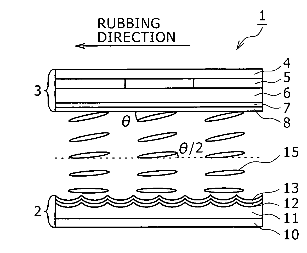
[0029]FIG. 1 is a sectional view showing, in a partly enlarged scale, a liquid crystal display panel 1 applied to a liquid crystal display apparatus of an Embodiment 1 of the present invention. The liquid crystal display apparatus of the present embodiment is of the transmission type or of the reflection type, and a polarizing plate and so forth are provided on a front side face of the liquid crystal display panel 1 which is the upper side in FIG. 1 or the like. In the transmission type, a backlight apparatus is provided on the rear face side of the liquid crystal display panel 1 which is the lower side in FIG. 1, but in the reflection type, a frontlight apparatus is provided on the front face side of the liquid crystal display panel 1 which is the upper side in FIG. 1.

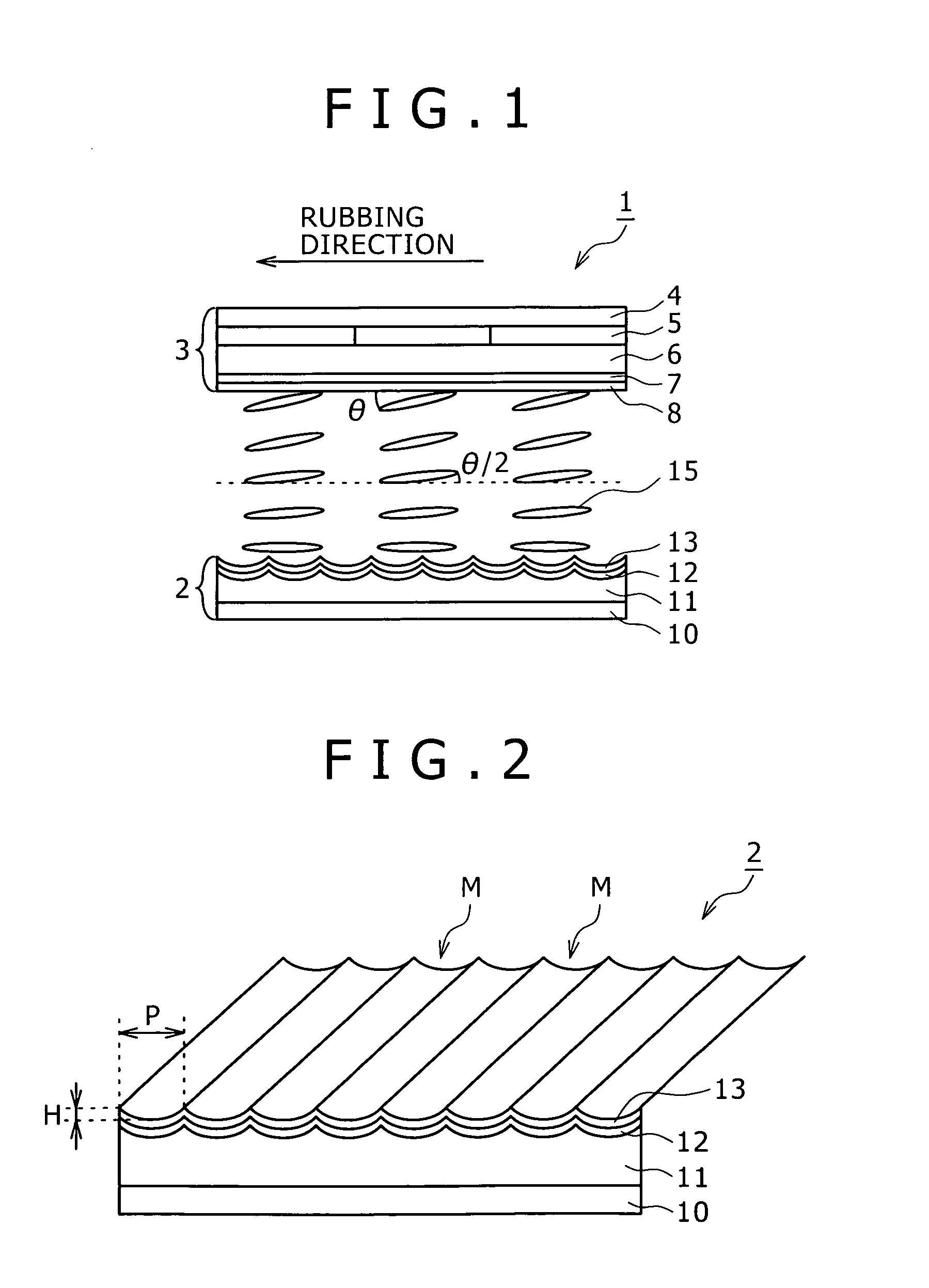
[0030]The liquid crystal display panel 1 includes liquid crystal sandwiched between a TFT array substrate 2 and a CF substrate 3. Here, the CF substrate 3 is produced b...

embodiment 2

[0058]FIG. 6 is a perspective view showing a TFT array substrate of a liquid crystal display panel applied to an Embodiment 2 of the present invention in contrast to FIG. 2. In this TFT array substrate 22, in place of the surface shape of the insulating film 11, the surface shape of the electrode 12 is formed in a groove shape while the shape of the face electrode 12 on which the orientation film 13 is produced is formed in a groove shape. The liquid crystal display panel of the present embodiment is formed similarly to the liquid crystal display panel 1 of the Embodiment 1 except the working of the groove shapes.

[0059]In particular, in the TFT array substrate 22 according to the present embodiment, the insulating film 11 is formed with a fixed film thickness on the glass substrate 10 in a similar manner as described hereinabove in connection with the Embodiment 1. Further, after a film of ITO, aluminum, silver or the like is formed subsequently, photosensitive resist is patterned i...

embodiment 3

[0061]FIG. 7 is a perspective view showing a TFT array substrate of a liquid crystal display panel applied to a liquid crystal display apparatus of an Embodiment 3 of the present invention in contrast to FIG. 2. This TFT array substrate 32 is configured such that, in place of the surface shape of the insulating film 11, the surface shape of the glass substrate 10 which is an insulating substrate is formed directly as a groove shape and the shape of the face of the glass substrate 10 on which the orientation film 13 is produced is formed in a groove shape. The liquid crystal display panel of the present embodiment is formed similarly to the liquid crystal display panel 1 of the Embodiment 1 except that it is different in terms of working of the groove shapes. It is to be noted that, although, in the example of FIG. 7, the insulating film is omitted, an insulating film may be provided as occasion demands.

[0062]In particular, in the TFT array substrate 32, after photosensitive resist o...


PUM

PropertyMeasurementUnit
depthaaaaaaaaaa
depthaaaaaaaaaa
thicknessaaaaaaaaaa

Abstract

The present invention relates to a liquid crystal display panel and a fabrication method for a liquid crystal display apparatus and makes it possible to assure high productivity when compared with related art apparatus and methods and assure sufficient anchoring strength and picture quality. In the present invention, the shape of a face on which an orientation film 13 is produced is set as a groove shape wherein a groove M extending in a predetermined direction is formed repetitively in a perpendicular direction to provide orientation ability to the orientation film 13.

Description

TECHNICAL FIELD[0001]This invention relates to a liquid crystal display panel and a fabrication method for a liquid crystal display apparatus and can be applied to a liquid crystal mode such as TN (Twisted Nematic), ECB (Electrically Controlled birefringence), STN (Super Twisted Nematic) and IPS (In-Plane Switching) modes. The present invention makes it possible to assure high productivity and sufficient anchoring strength and picture quality when compared with related art apparatus and methods by providing a lower face of an orientation film with a groove shape to provide orientation ability to the orientation film.BACKGROUND ART[0002]Conventionally, in liquid crystal display panels of various liquid crystal modes such as TN, ECB, STN and IPS modes, liquid crystal molecules are oriented to a fixed direction by an orientation process, and various techniques have been proposed for this orientation process.[0003]Here, a rubbing method which is one of such orientation processes is a me...

Claims


Application Information

Patent Timeline
Patent Type & Authority Applications(United States)
IPC IPC(8): G02F1/1337G02F1/13G02F1/13363
CPCG02F1/133345G02F1/133707G02F2001/133776G02F1/133784G02F2001/133757G02F1/133753G02F1/133757G02F1/133776G02F1/1333G02F1/13363G02F1/1337
Inventor TAMAKI, MASAYA
Owner SONY CORP
Why Eureka
Try Eureka