
Plasma doping with enhanced charge neutralization

a technology of charge neutralization and plasma doping, which is applied in the field of plasma doping with enhanced charge neutralization, can solve the problems of device damage, non-uniform doping, and poor process control of plasma doping systems

Inactive Publication Date: 2009-01-01
VARIAN SEMICON EQUIP ASSOC INC
View PDF8 Cites 44 Cited by
  • Summary
  • Abstract
  • Description
  • Claims
  • Application Information

AI Technical Summary

Benefits of technology

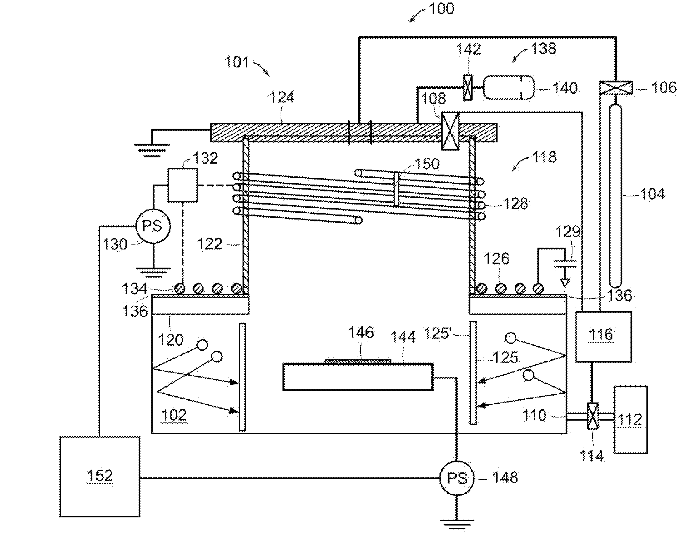
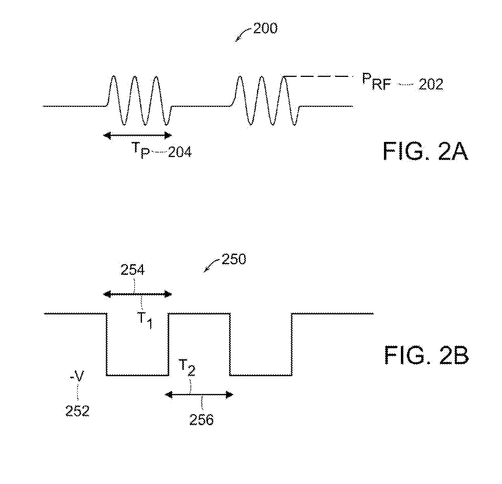
The present invention relates to a system and method for plasma doping, which is a process used in the semiconductor and other industries for doping materials with ions. The invention aims to improve the process control of plasma doping systems by reducing the non-uniformity of doping and the development of charge build-up on the substrate being plasma doped. The invention provides a waveform that can neutralize charge accumulation on the substrate and a method for applying a negative voltage to the substrate to attract ions for implantation. The invention also includes various alternatives, modifications, and equivalents for use in plasma doping systems.

Problems solved by technology

In general, the process control of plasma doping systems is not as good as conventional beam-line ion implantation systems.
This charge build-up can result in the development of a relatively high potential voltage on the substrate that can cause doping non-uniformities, arcing, and device damage.

Method used


Image

  • Plasma doping with enhanced charge neutralization
  • Plasma doping with enhanced charge neutralization
  • Plasma doping with enhanced charge neutralization

Examples


Embodiment Construction

[0015]Reference in the specification to “one embodiment” or “an embodiment” means that a particular feature, structure, or characteristic described in connection with the embodiment is included in at least one embodiment of the invention. The appearances of the phrase “in one embodiment” in various places in the specification are not necessarily all referring to the same embodiment.

[0016]It should be understood that the individual steps of the methods of the present invention may be performed in any order and / or simultaneously as long as the invention remains operable. Furthermore, it should be understood that the apparatus and methods of the present invention can include any number or all of the described embodiments as long as the invention remains operable.

[0017]The present teachings will now be described in more detail with reference to exemplary embodiments thereof as shown in the accompanying drawings. While the present teachings are described in conjunction with various embod...


PUM

PropertyMeasurementUnit
dielectric constantaaaaaaaaaa
power levelaaaaaaaaaa
bias voltageaaaaaaaaaa

Abstract

A plasma doping apparatus includes a pulsed power supply that generates a pulsed waveform having a first period with a first power level and a second period with a second power level. A plasma source generates a pulsed plasma with the first power level during the first period and with the second power level during the second period. A bias voltage power supply generates a bias voltage waveform at an output that is electrically connected to a platen which supports a substrate. The bias voltage waveform having a first voltage during a first period and second voltage with a negative potential that attract ions in the plasma to the substrate for plasma doping during a second period. At least one of the first and second power levels of the RF waveform is chosen to at least partially neutralize charge accumulating on the substrate.

Description

[0001]The section headings used herein are for organizational purposes only and should not to be construed as limiting the subject matter described in the present application.BACKGROUND OF THE INVENTION[0002]Plasma processing has been widely used in the semiconductor and other industries for many decades. Plasma processing is used for tasks such as cleaning, etching, milling, and deposition. More recently, plasma processing has been used for doping. Plasma doping is sometimes referred to as PLAD or plasma immersion ion implantation (PIII). Plasma doping systems have been developed to meet the doping requirements of some modern electronic and optical devices.[0003]Plasma doping is fundamentally different from conventional beam-line ion implantation systems that accelerate ions with an electric field and then filter the ions according to their mass-to-charge ratio to select the desired ions for implantation. In contrast, plasma doping systems immerse the target in a plasma containing ...

Claims


Application Information

Patent Timeline
Patent Type & Authority Applications(United States)
IPC IPC(8): H01L21/26C23C16/00H05H1/24
CPCH01J37/321H01J37/32165H01L21/32136C23C14/345H01J37/32412
Inventor SINGH, VIKRAMMILLER, TIMOTHYLINDSAY, BERNARD
Owner VARIAN SEMICON EQUIP ASSOC INC
Learn More