Method for fabricating interconnection in semiconductor device

Inactive Publication Date: 2009-01-01
SK HYNIX INC
View PDF44 Cites 21 Cited by
  • Summary
  • Abstract
  • Description
  • Claims
  • Application Information

AI Technical Summary

Problems solved by technology

The boron ions in the boron layer can penetrate a semiconductor substrate, thereby causing degradation in electrical properties of a semiconductor device.
Further,

Method used


Image

  • Method for fabricating interconnection in semiconductor device
  • Method for fabricating interconnection in semiconductor device
  • Method for fabricating interconnection in semiconductor device

Examples


Embodiment Construction

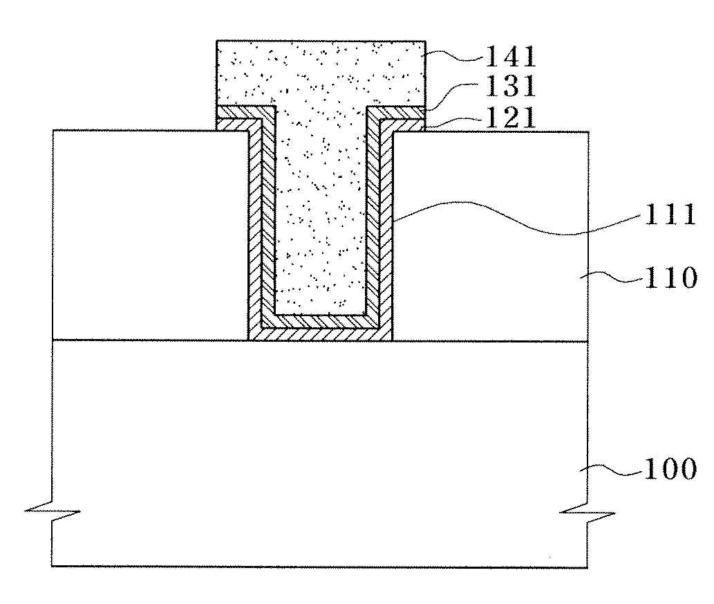
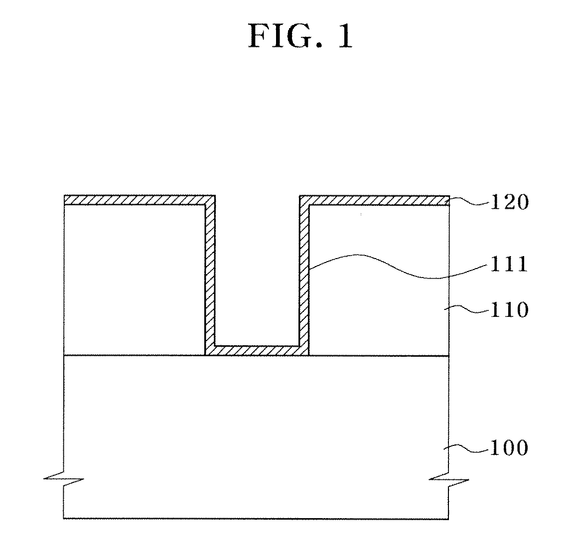
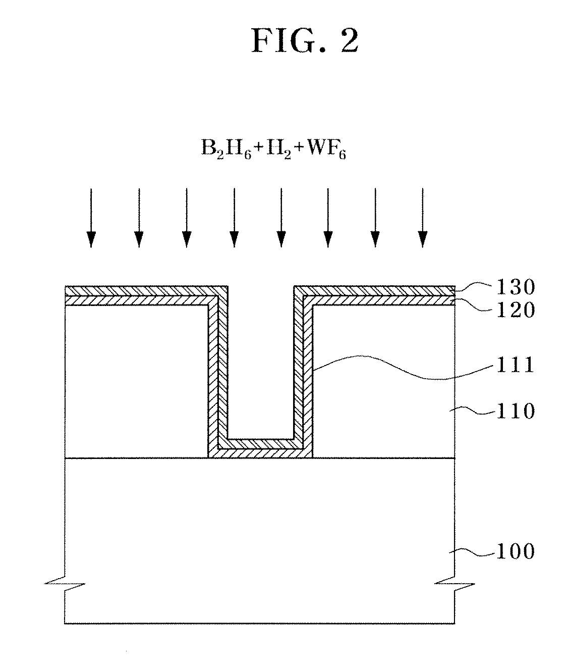
[0011]Hereinafter, a method for fabricating an interconnection in a semiconductor device according to the present invention will be described in detail with reference to the accompanying drawings.

[0012]FIGS. 1 to 4 illustrate a method for fabricating an interconnection in a semiconductor device according to one embodiment of the present invention.

[0013]Referring to FIG. 1, an interlayer dielectric layer 110 is formed on a semiconductor substrate 100 having a lower structure (not shown). For example, in a memory device such as DRAM, prior to the formation of the interlayer dielectric layer 110, an isolation layer is formed by a shallow trench isolation (STI) process. The isolation layer defines an active region in the semiconductor substrate 100. Then, a transistor including a source / drain region and a gate electrode may be formed in the active region of the semiconductor substrate 100.

[0014]The interlayer dielectric layer 110 is selectively etched to form a bit line contact hole 111...


PUM


Abstract

A method for fabricating an interconnection in a semiconductor device includes forming a hydrogenated tungsten nucleation layer on a semiconductor substrate, and forming a bulk tungsten layer on the tungsten nucleation layer. Boron ions react with a hydrogen gas supplied together with a diborane gas to be restored to a diborane again, thereby preventing a boron layer from being formed on an interface of the tungsten nucleation layer.

Description

CROSS-REFERENCE TO RELATED APPLICATIONS[0001]Priority to Korean Patent application number 10-2007-0064756, filed on Jun. 28, 2007, the disclosure of which is hereby incorporated by reference herein in its entirety, is claimed.BACKGROUND OF THE INVENTION[0002]The present invention relates to a method for fabricating a semiconductor device, and more particularly, to a method for fabricating an interconnection in a semiconductor device.[0003]As the minimum line width of a semiconductor device decreases, resistances of a contact plug or an ohmic contact increases. In fabrication of a semiconductor device, a metal interconnection or bit line is frequently formed of tungsten which has a low resistivity. Tungsten has been used for the ohmic contact and bit line so as to compensate for the increase in resistance due to the reduction of the bit line width and to reduce a sheet resistance. Therefore, much research has been conducted to reduce the resistance of tungsten.[0004]As one example, t...

Claims


Application Information

Patent Timeline
IPC IPC(8): H01L21/4763
CPCH01L21/2855H01L21/76877H01L21/76876H01L21/28556H01L21/28
Inventor KIM, CHOON HWANRHO, II CHEOL
Owner SK HYNIX INC
Why Eureka
Try Eureka