Method and system for enhancing the yield in semiconductor manufacturing

a technology of semiconductor manufacturing and yield enhancement, applied in the direction of program control, total factory control, instruments, etc., can solve the problems of increasing the subjectivity of yield to other limiting factors, difficult control of process steps, and high cost, so as to improve the accuracy of physical modeling, the effect of increasing complexity and loss of accuracy

Active Publication Date: 2009-01-01
SYNOPSYS INC
View PDF3 Cites 26 Cited by
  • Summary
  • Abstract
  • Description
  • Claims
  • Application Information

AI Technical Summary

Benefits of technology

[0027]The use of TCAD Process Compact Models over the TCAD Process Model can have considerable advantages over the direct use of TCAD, even though there is an approximation error and therefore a loss of accuracy involved. TCAD tools are typically very complex, with the complexity rising with the growing accuracy of physical modeling. In practice, TCAD simulations take considerable time to perform. In addition, TCAD tools due to their complexity are in general sufficiently robust for a research and development environment, but not for a production environment. TCAD Process Compact Models, on the other side, have much less complexity, are therefore much more robust towards program failures, and can be evaluated in a much shorter time. As an example, a typical 2-dimensional process and device simulation using TCAD currently takes typically one hour, whereas a TCAD Process Compact Model can typically be evaluated in less than a microsecond. The disadvantage of the process compact model is that only the predefined output parameters are available, whereas each TCAD simulation typically generates a comprehensive representation of a semiconductor device that can subsequently be examined and probed in arbitrary ways. In the present targeted application, the latter is typically not required, and the TCAD Process Compact Model has therefore considerable practical advantages.

Problems solved by technology

This is as opposed to real experiments, where the control of process steps may be difficult and subject to uncontrollable drift or variation in the equipment, and where the limitations of metrology can make it difficult, expensive or impossible to make measurements both in non-destructive and destructive measurements.
In this range the yield is increasingly subject to other limiting factors than just defects.
Unfortunately, while TCAD simulations can be made very accurate, they are still very time consuming to execute.
This deficiency severely limits the practicality of using TCAD in manufacturing, as opposed to design and development.
Each of the experiments will usually take a considerable amount of time, as previously mentioned.
Although there is generally a certain loss of accuracy incurred by using an approximation function, an appropriate choice of “Design of Experiment” and an appropriate choice of approximation function can bring down the error to a reasonably small amount.
TCAD tools are typically very complex, with the complexity rising with the growing accuracy of physical modeling.
In practice, TCAD simulations take considerable time to perform.
In addition, TCAD tools due to their complexity are in general sufficiently robust for a research and development environment, but not for a production environment.
The disadvantage of the process compact model is that only the predefined output parameters are available, whereas each TCAD simulation typically generates a comprehensive representation of a semiconductor device that can subsequently be examined and probed in arbitrary ways.
As no manufacturing process is perfect, the products obtained in real manufacturing are subject to manufacturing defects or their performance differs from the targeted results, resulting in non-optimum defect yield and non-optimum systematic yield.
In semiconductor manufacturing, this problem of process defects and process variability is generally increasing with smaller technologies.
Some drawbacks of existing techniques arethat the known models for controlling and correcting processes at this point are very limited in their applicability, by not being able to encompass a sufficiently high number of process parameters and their interactions, or by not being able to accommodate the nonlinearity of some parameters.that creating process models or process compact models from purely experimental data requires costly experiments.that not all process parameters can be measured at all or at reasonable cost and are therefore not amenable to conventional process control and yield managementthat not all product performance parameters can be measured at all or measured at reasonable cost, and are therefore not amenable to conventional process control and yield management.

Method used


Image

  • Method and system for enhancing the yield in semiconductor manufacturing
  • Method and system for enhancing the yield in semiconductor manufacturing
  • Method and system for enhancing the yield in semiconductor manufacturing

Examples


Embodiment Construction

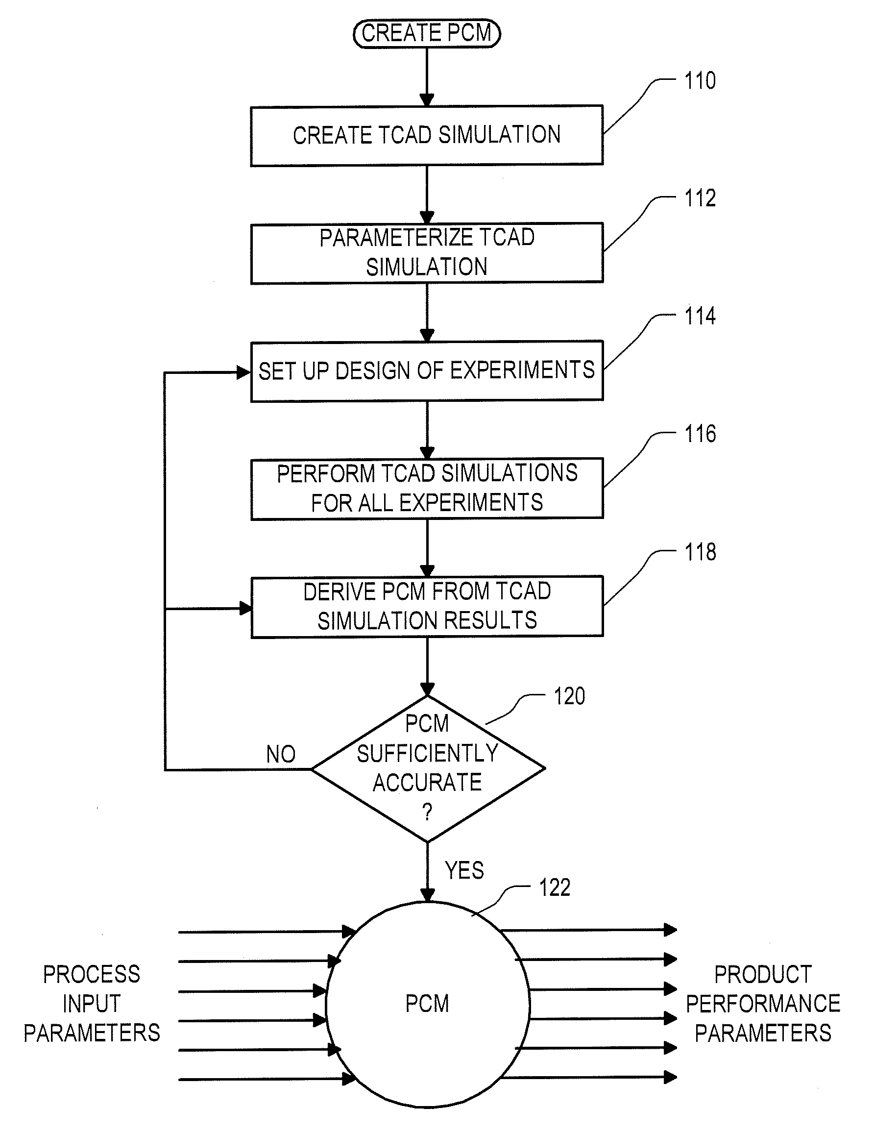
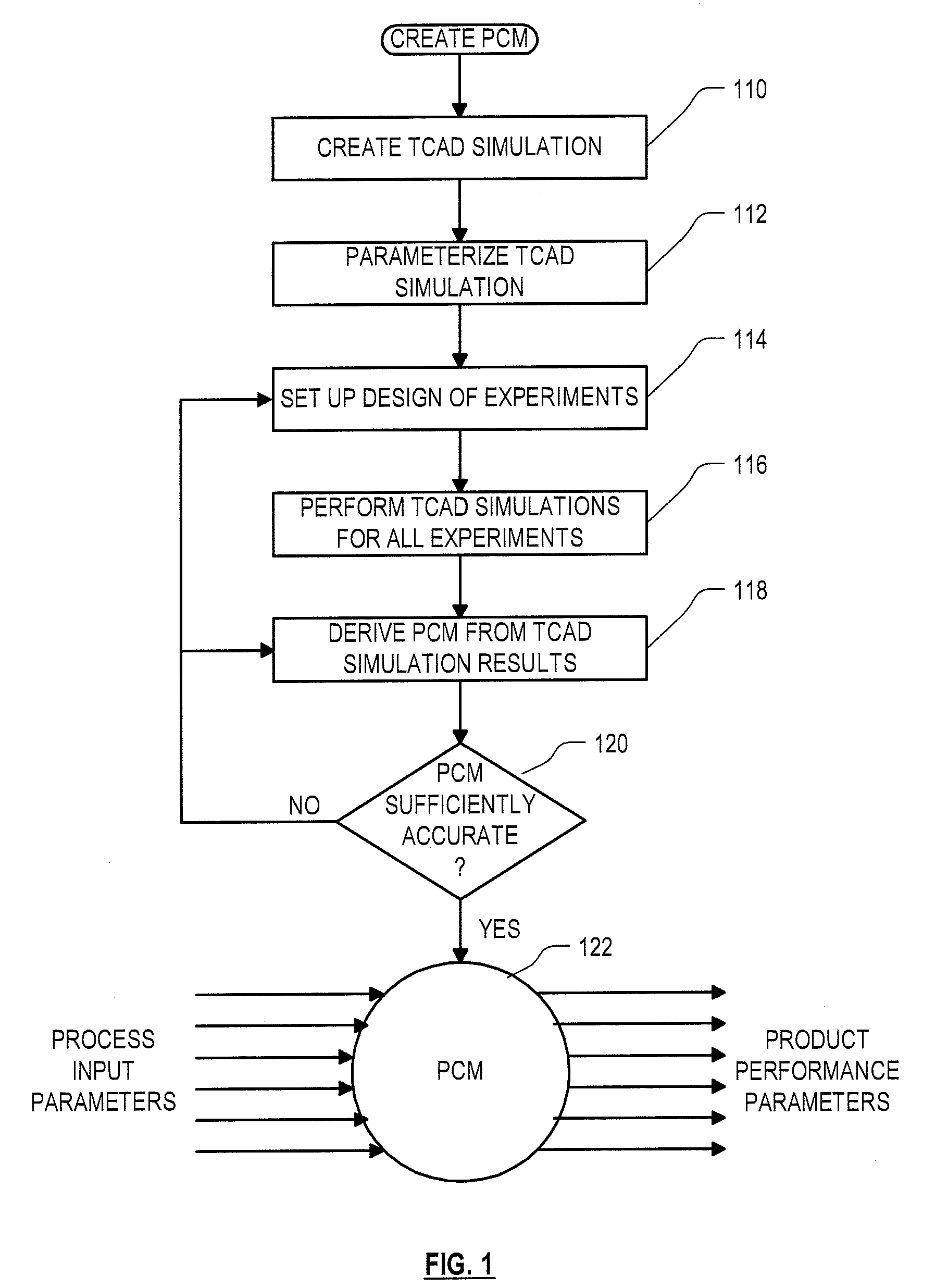
[0037]The following description is presented to enable any person skilled in the art to make and use the invention, and is provided in the context of a particular application and its requirements. Various modifications to the disclosed embodiments will be readily apparent to those skilled in the art, and the general principles defined herein may be applied to other embodiments and applications without departing from the spirit and scope of the present invention. Thus, the present invention is not intended to be limited to the embodiments shown, but is to be accorded the widest scope consistent with the principles and features disclosed herein.

[0038]In FIG. 1, a PCM 122 is shown together with its process parameter inputs and its product performance parameter outputs. The PCM can be used in a variety of different ways to enhance the manufacturing process. In various different use scenarios, actual or desired values are provided for some of the parameters, and actual or desired values ...


PUM


Abstract

Roughly described, a manufacturing process is enhanced by using TCAD and TCAD-derived models. A TCAD simulation model of the process is developed, which predicts, in dependence upon a plurality of process input parameters, a value for a performance parameter of a product to be manufactured using the process. Estimated, predicted or desired values for a calculated subset of the parameters (including either process input parameters or product performance parameters or both), are determined in dependence upon the process model, and further in dependence upon actual, estimated or desired values for a different subset of the parameters (again either process input parameters or product performance parameters or both). The determination is preferably made using a process compact model of the process, itself developed in dependence upon the simulation model.

Description

CROSS-REFERENCES[0001]This application is a Continuation of U.S. patent application Ser. No. 11 / 139,110 filed 27 May 2005, which is a Continuation-In-Part of U.S. patent application Ser. No. 11 / 092,967 filed 29 Mar. 2005, which claims the benefit of Provisional Application No. 60 / 557,382 filed 30 Mar. 2004. All parent applications are incorporated herein by reference in their entirety.1. FIELD OF THE INVENTION[0002]The invention relates to a method for enhancing the yield in semiconductor manufacturing, a computer program product and a system for enhancing the yield in semiconductor manufacturing.2. BACKGROUND AND SUMMARY OF THE INVENTION[0003]Technology Computer Aided Design (TCAD) uses physics-based computer simulations to design, analyze, and optimize semiconductor devices. TCAD represents the available physical knowledge of semiconductor processing and devices in terms of computer models. It represents devices as one dimensional, two-dimensional or threedimensional finite-elemen...

Claims


Application Information

Patent Timeline
Patent Type & Authority Applications(United States)
IPC IPC(8): G06F19/00G06G7/66
CPCG05B19/41885G05B2219/32017G06F2217/80G06F17/5009G05B2219/45031G06F2119/08G06F30/20Y02P90/02G03F7/705
Inventor BOMHOLT, LARSCHALMERS, JIMFICHTNER, WOLFGANG
Owner SYNOPSYS INC
Why Eureka
Try Eureka