Solderable EMI Gasket and Grounding Pad

a technology of grounding pads and gaskets, which is applied in the field of grounding pads and electrically conductive gaskets, can solve the problems of increasing complexity of electronic circuits, increasing difficulty in solving problems, and scarce pcb real estate available, so as to improve the surface conductivity of invention, improve the flexibility of part shapes, and increase the surface area

Inactive Publication Date: 2009-01-08
WL GORE & ASSOC INC
View PDF18 Cites 23 Cited by
  • Summary
  • Abstract
  • Description
  • Claims
  • Application Information

AI Technical Summary

Benefits of technology

[0007]The present invention improves on the previous concepts by providing an SMT compatible grounding pad that has an inherently solderable surface. In this concept, the shim support layer is not needed to provide the interface between the conductive gasket material and the solder bond to the PCB ground trace. This approach allows for more flexibility in part shapes, lengths and geometries. The base material is comprised of a metal filled elastomer, or composite of a metal filled elastomer with another elastomer. The outside of the base material is then applied a continuous coating of metallization. The outer metal can be deposited by electroless plating or electrolytic plating technologies, or by vapor deposition of the metal, or any combination of these techniques. This outer metal layer provides a solderable surface for the solder paste to adhere to and attach to the ground trace of the PCB. It will also improve the surface conductivity of the invention by providing more surface area to connect to the corresponding component, shield, or chassis.

Problems solved by technology

These trends generate increasingly complex electronic circuits forcing designers to put more components per square inch onto the printed circuit board (PCB).
This yields densely populated circuits, where available PCB real estate is becoming a scarce commodity.
With so many circuit elements being densely populated and cohabitating on the same PCB, the circuit designer is now faced with the challenge of providing shielding for the different circuits which are in such close proximity to each other.
This challenge is made more difficult by the fact that available real-estate on the PCB where the shields would normally be attached is continually shrinking.
The challenge for this technique is how to electrically and mechanically attach the shield to the board.
Although these technologies offer designers creative options for solving densely populated PCB shielding problems, they still require some design and tooling efforts in order to integrate them into the PCB assembly.
SMT compatible metal clips have been used in similar applications but suffer from potential damage, due to lack of robustness, and limited grounding, due to small surface area of the contact points.
In this case the only path for current flow is through the metallization itself, which may become cracked or damaged with flexing and use, and thus provides an unreliable device.

Method used


Image

  • Solderable EMI Gasket and Grounding Pad
  • Solderable EMI Gasket and Grounding Pad
  • Solderable EMI Gasket and Grounding Pad

Examples


Embodiment Construction

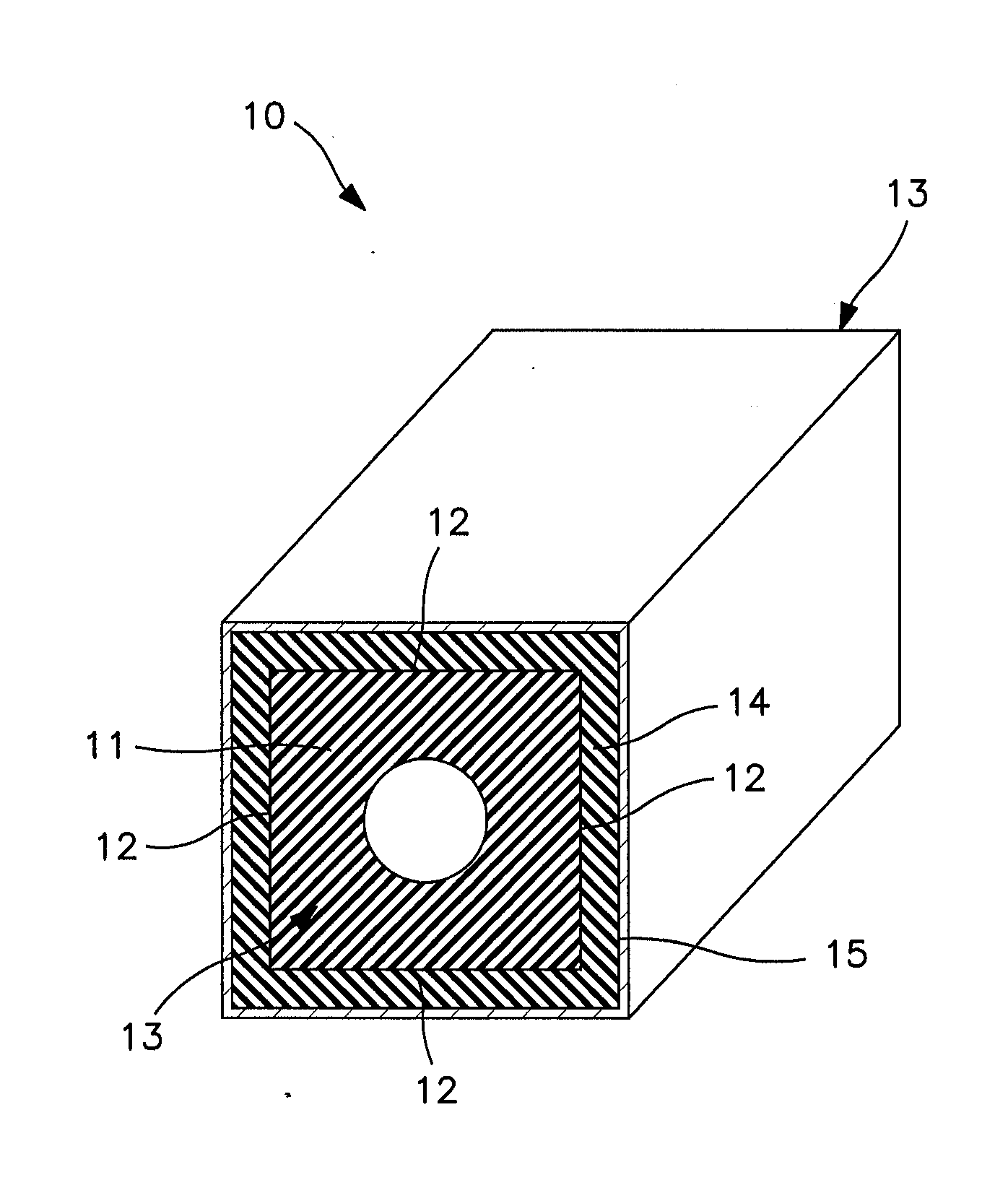
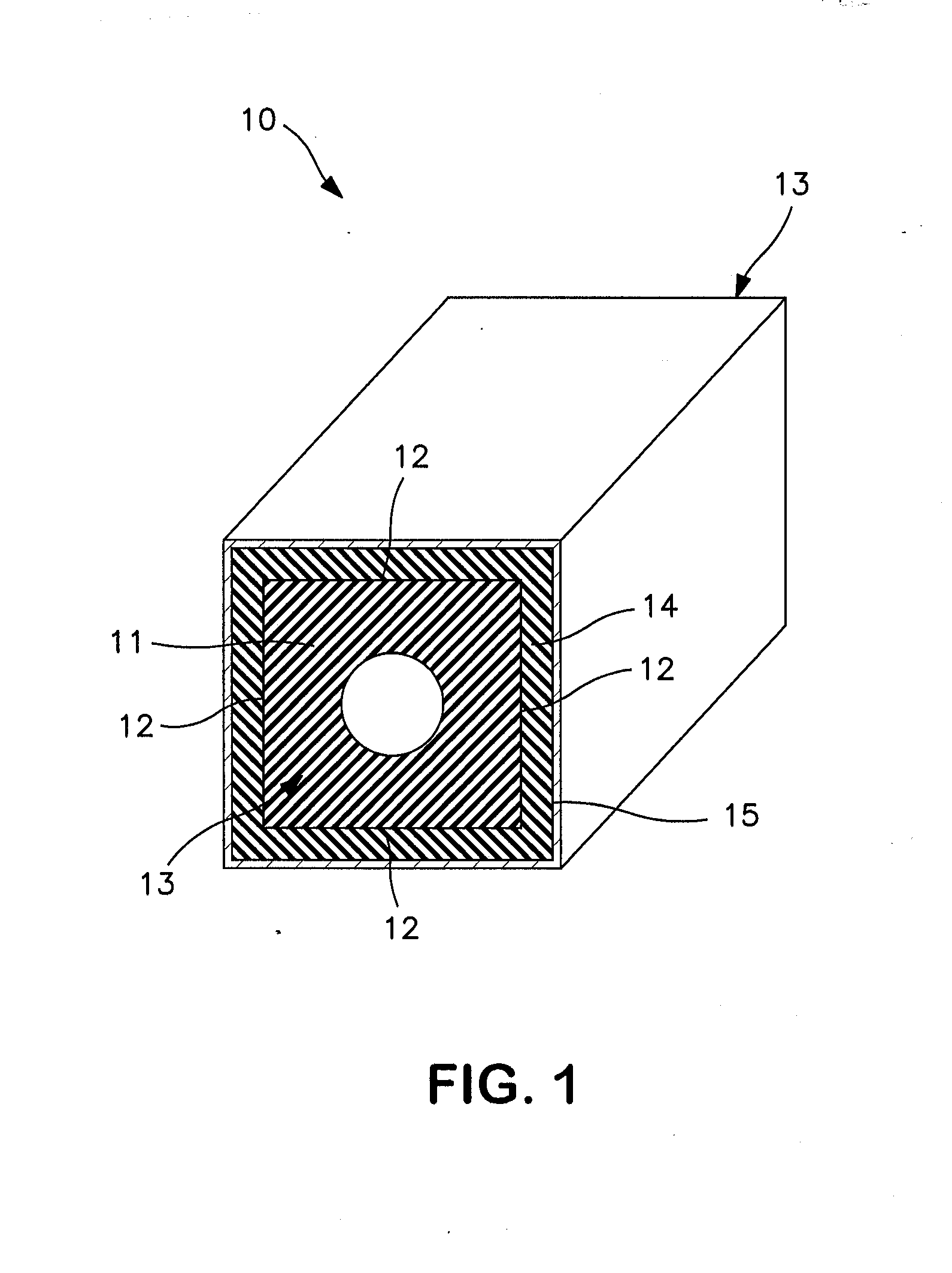
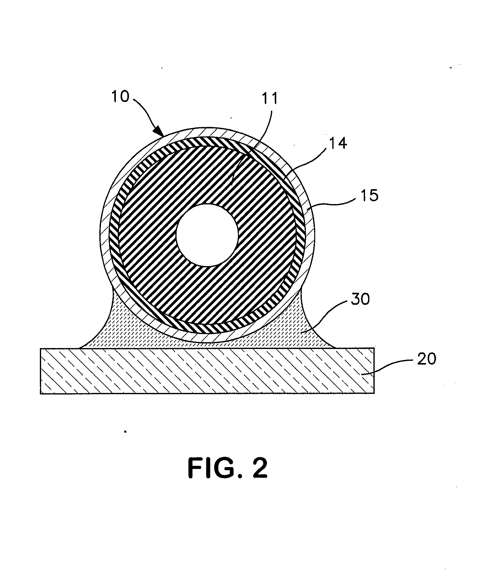
[0018]A preferred embodiment of the present invention is illustrated in FIG. 1. FIG. 1 shows an apparatus 10. Apparatus 10 can be either a grounding pad or a gasket. Typically, when used as a gasket, apparatus 10 is dispersed at a plurality of locations around, for example, a circuit board to create an interface between the PCB and the shield to form a Faraday cage to prevent EMI radiation being emitted from components on the circuit board. When used as a grounding pad, one or more of apparatus 10 may be disposed at various locations on, for example, a circuit board, to provide grounding locations for desired electrical performance. Apparatus 10 comprises a compressible elastomeric substrate 11. As used herein, compressible means compressible to 75% of its original (or uncompressed) height with an applied load of less than 500 pounds per square inch when compressed between two steel plates on a load frame at a rate of 1 mm per minute.

[0019]Compressible elastomeric substrate 11 has a...


PUM

PropertyMeasurementUnit
lengthaaaaaaaaaa
lengthaaaaaaaaaa
compressibleaaaaaaaaaa

Abstract

Apparatus, which is useful as both a conductive gasket and a grounding pad, which has a compressible elastomeric substrate having at least one side surface and two ends, a conductive elastomeric layer adjacent to all of the side surfaces of the compressible substrate, and a metal layer adjacent to the conductive layer.

Description

FIELD OF THE INVENTION[0001]This invention relates to grounding pads and electrically conductive gaskets, and in particular to such a device that is compressible and solderable.BACKGROUND OF THE INVENTION[0002]“Signal Integrity” is a term used in the high-speed digital world to describe the management of primary or “wanted” signals in the transmission path. EMC, or Electromagnetic Compatibility, usually describes the management of “unwanted” signals in an electronic circuit or system. Traditionally, circuits were placed in metal enclosures creating a “Faraday cage” effect that would shield the electronic circuit or system from any unwanted signals. Conversely, the shield would prevent any wanted signals from escaping the enclosure.[0003]Modern electronics have experienced trends such as the increased usage of handheld devices, higher wireless bandwidth, and faster computing speeds. These trends generate increasingly complex electronic circuits forcing designers to put more component...

Claims


Application Information

Patent Timeline
Patent Type & Authority Applications(United States)
IPC IPC(8): B23K31/02F16J15/06H05K9/00B05D3/12
CPCH05K9/0015
Inventor ZONVIDE, KOSSITRETHEWEY, JEREMY
Owner WL GORE & ASSOC INC
Why Eureka
Try Eureka