

Semiconductor device and method for manufacturing the same
- Summary
- Abstract
- Description
- Claims
- Application Information
AI Technical Summary
Benefits of technology
Problems solved by technology
Method used
Image

Examples
embodiment mode 1
[0041]This embodiment mode describes an example of a method for manufacturing a semiconductor device of the present invention, with reference to FIGS. 1A to 1D, FIGS. 2A to 2D, FIGS. 3A to 3D, FIGS. 4A to 4C, FIGS. 5A to 5C, FIGS. 6A to 6C, and FIGS. 7A to 7C.
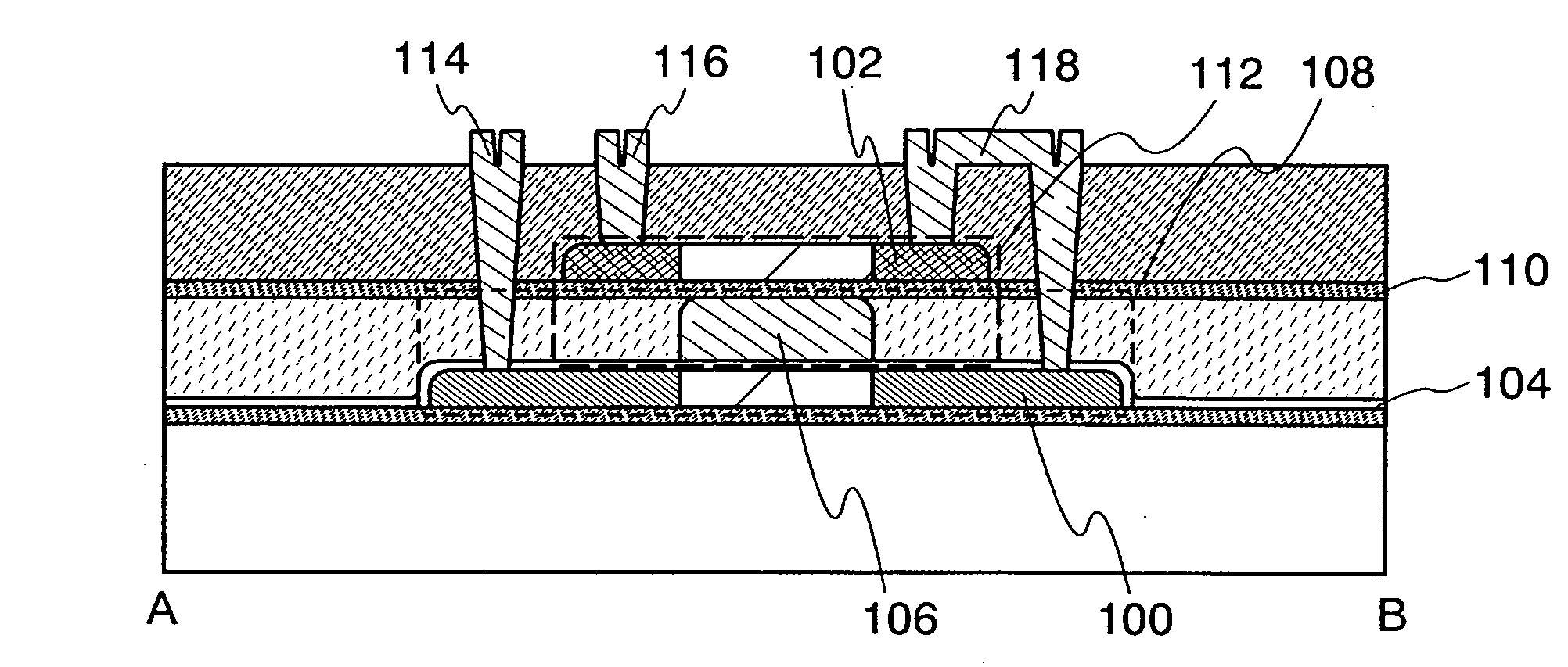
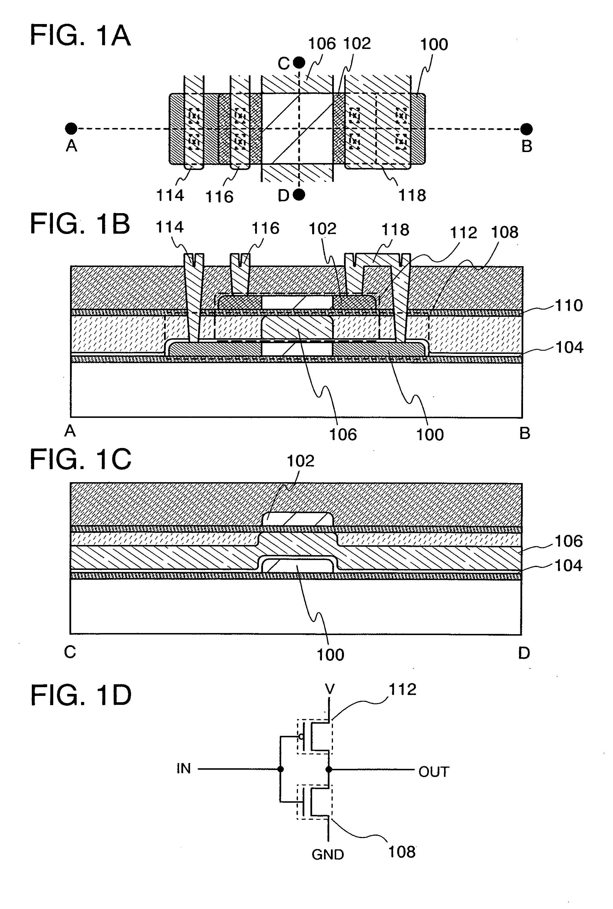
[0042]FIGS. 1A to 1D illustrate an example of a structure of a semiconductor device of the present invention. FIG. 1A is a plan view of a semiconductor device of the present invention. FIG. 1B is a cross-sectional view taken along line A-B in FIG. 1A, and FIG. 1C is a cross-sectional view taken along line C-D in FIG. 1A. The structure shown in FIGS. 1A to 1D is just an example, and the present invention is not limited to the structure.
[0043]The semiconductor device illustrated in FIGS. 1A to 1D includes two single-crystal semiconductor layers (a single-crystal semiconductor layer 100 and a single-crystal semiconductor layer 102). A first transistor 108 includes the single-crystal semiconductor layer 100 as well as an insulating...
embodiment mode 2
[0097]This embodiment mode describes another example of a method for manufacturing a semiconductor device of the present invention, with reference to FIGS. 8A to 8D, FIGS. 9A to 9D, FIGS. 10A to 10C, FIGS. 11A to 11C, FIGS. 12A to 12C, and FIGS. 13A to 13C. Note that in this embodiment mode, the detailed description where Embodiment Mode 1 can be referred to is omitted.
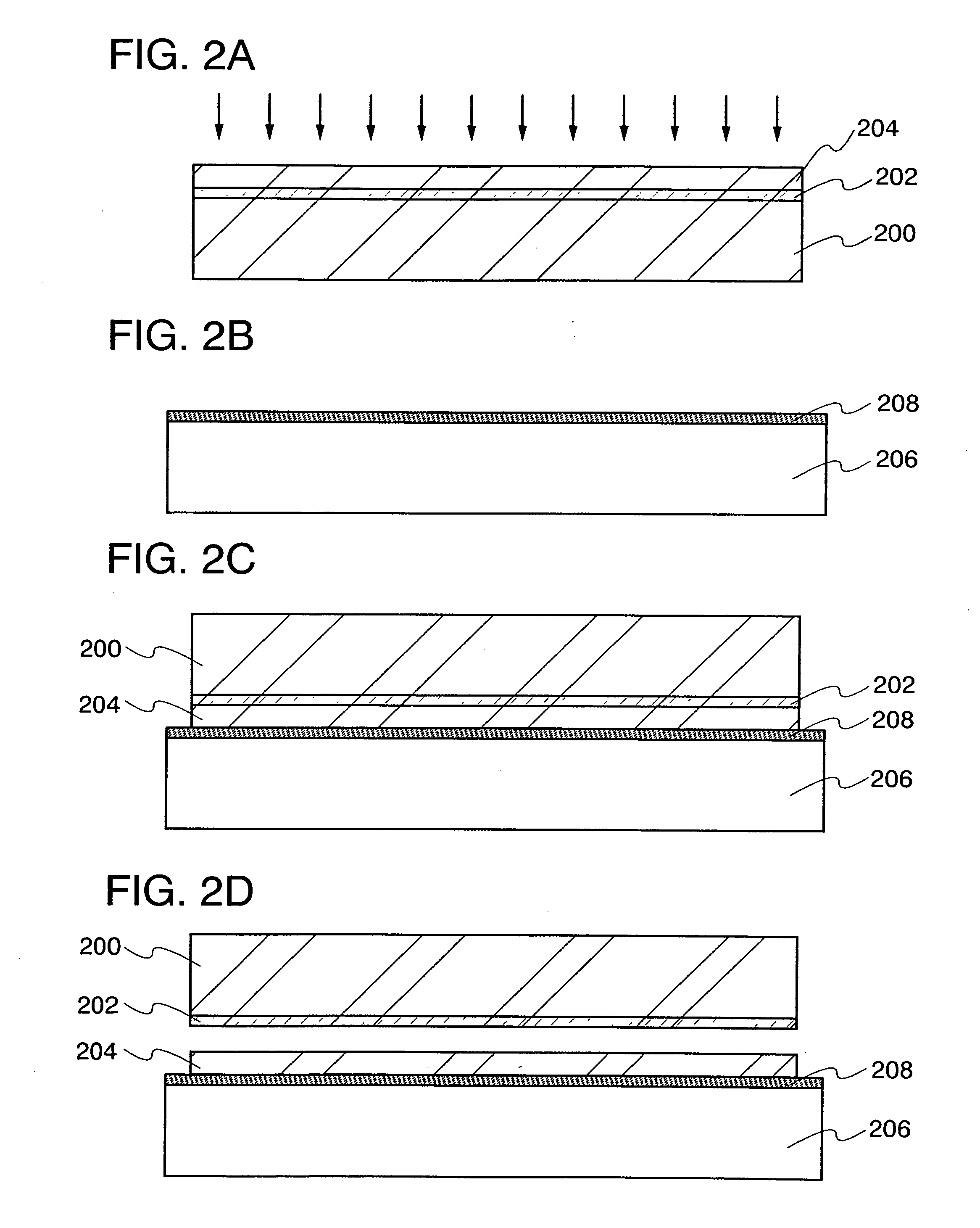
[0098]First, a single-crystal semiconductor substrate 800 is prepared. Ions are introduced to a predetermined depth from a surface of the single-crystal semiconductor substrate 800 to form a damaged region 802 and a single-crystal semiconductor layer 804 (see FIG. 8A). The detailed description on a method for forming the damaged region 802 and the single-crystal semiconductor layer 804 is omitted here, because Embodiment Mode 1 can be referred to.
[0099]The single-crystal semiconductor substrate 800 is not particularly limited as long as it is a substrate made of a single-crystal semiconductor material. In this embodim...
embodiment mode 3
[0135]This embodiment mode will describe an example of a semiconductor device of the present invention, with reference to FIGS. 14A and 14B. Note that although description will be made by using a liquid crystal display device as an example of a semiconductor device in this embodiment mode, a semiconductor device which can be manufactured according to the present invention is not limited to a liquid crystal display device.
[0136]FIGS. 14A and 14B show an example of a liquid crystal display device of the present invention. FIG. 14A is a plan view of a liquid crystal display device, and FIG. 14B is a cross-sectional view taken along line E-F in FIG. 14A. The liquid crystal display device can be manufactured in the following manner: after a transistor is formed over a substrate 1400 having an insulating surface by using a method described in Embodiment Mode 1, Embodiment Mode 2, or the like, an interlayer insulating layer 1402, a pixel electrode 1404, a spacer 1406, an insulating layer 1...
PUM
 Abstract
Description
Claims
Application Information