
Semiconductor device

Active Publication Date: 2013-06-27
SEMICON ENERGY LAB CO LTD
View PDF1 Cites 39 Cited by
  • Summary
  • Abstract
  • Description
  • Claims
  • Application Information

AI Technical Summary

Benefits of technology

The invention aims to create a semiconductor device that can have high productivity and yield while keeping the number of steps and layers low. Additionally, the device should have a small area and low power consumption. This means that even when transistors overlap with each other, the device should be highly productive and yielding.

Problems solved by technology

In the case where a transistor using an oxide semiconductor film overlaps with another transistor, however, the number of steps and layers increases, which might cause a decrease in yield due to complicated manufacturing process.

Method used


Image

  • Semiconductor device
  • Semiconductor device
  • Semiconductor device

Examples


embodiment 1

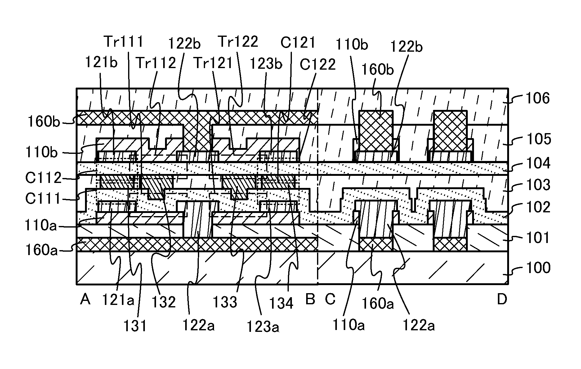
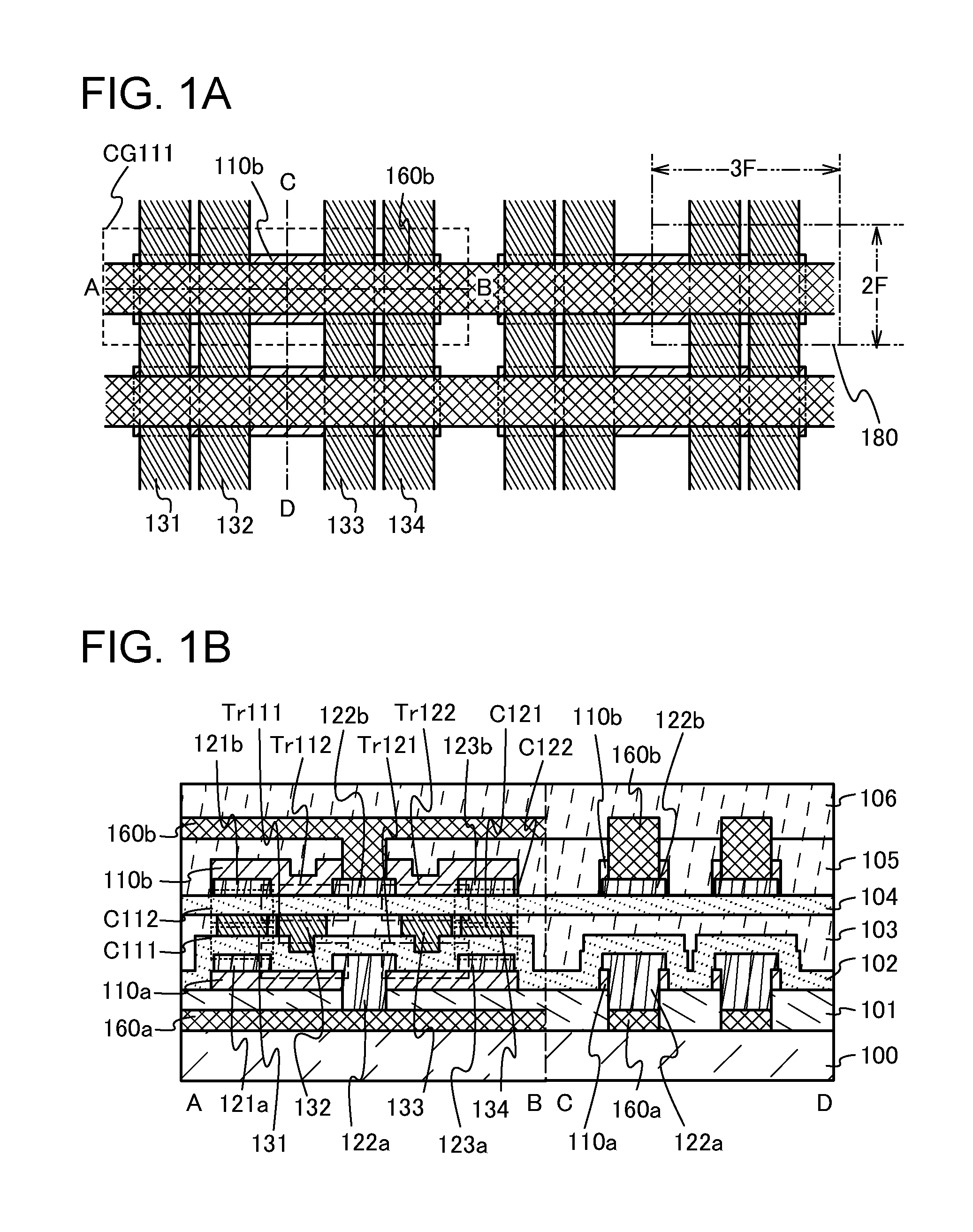
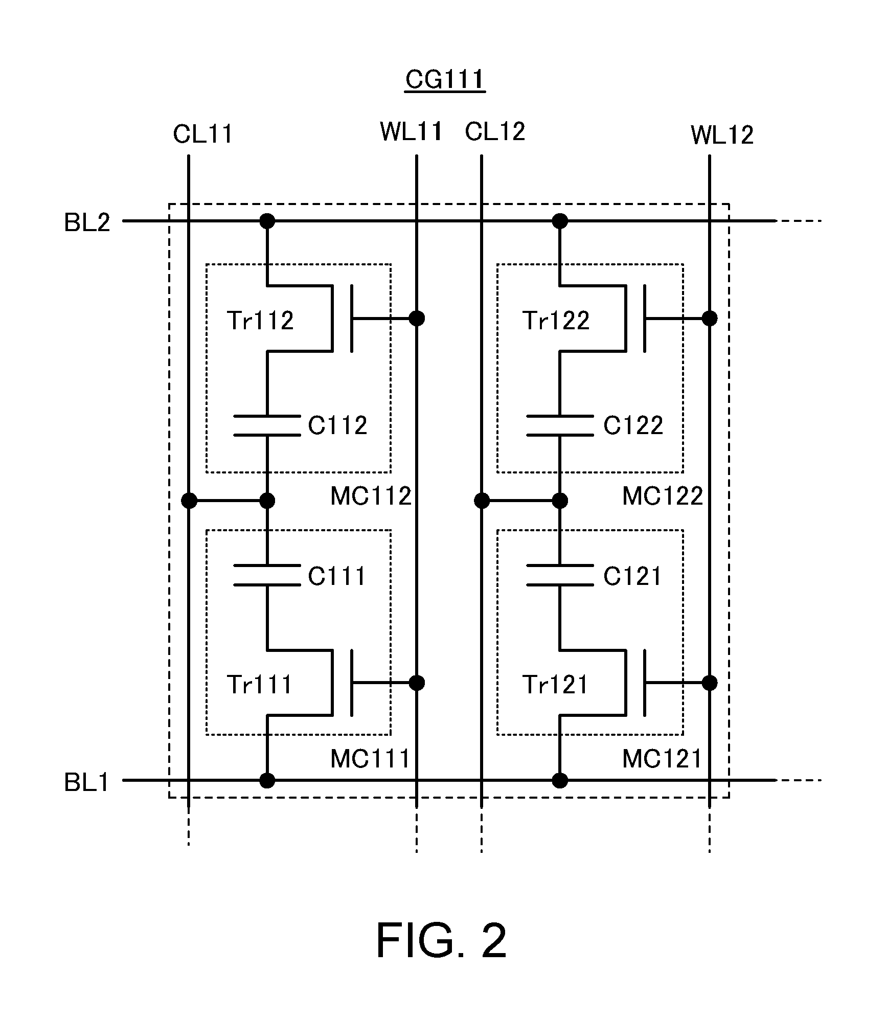
[0044]In this embodiment, an example of a semiconductor device of one embodiment of the present invention will be described with reference to FIGS. 1A and 1B, FIG. 2, FIGS. 3A to 3E, FIGS. 4A to 4D, FIGS. 5A to 5C, FIGS. 6A to 6C, and FIGS. 7A and 7B.

[0045]FIG. 1A is a top view of the semiconductor device of one embodiment of the present invention. FIG. 1B illustrates a cross-section A-B and a cross-section C-D corresponding to a dashed-dotted line A-B and a dashed-dotted line C-D of FIG. 1A, respectively. In FIG. 1A, films, insulating films, and the like which overlap with each other are omitted for simplicity.

[0046]The semiconductor device illustrated in FIG. 1B includes the following: a conductive film 160a provided over a substrate 100; an insulating film 101 which has an opening reaching the conductive film 160a and is provided over the substrate 100 and the conductive film 160a; a semiconductor film 110a which has an opening reaching the conductive film 160a and is provided ov...

embodiment 2

[0156]In this embodiment, a semiconductor device will be described with reference to

[0157]FIG. 8, FIG. 9, and FIG. 10, the semiconductor device including a plurality of structures of semiconductor device described in Embodiment 1 which overlap with each other.

[0158]FIG. 8 is a cross-sectional view of the semiconductor device shown in this embodiment. Since a top view of the semiconductor device is the same as FIG. 1A except for reference numerals, description thereof is omitted. FIG. 8 illustrates a cross-section A-B and a cross-section C-D corresponding to the dashed-dotted line A-B and the dashed-dotted line C-D of FIG. 1A, respectively.

[0159]In the semiconductor device in FIG. 8, a conductive film 260a corresponds to the conductive film 160a, a conductive film 231a corresponds to the conductive film 131, a conductive film 232a corresponds to the conductive film 132, a conductive film 233a corresponds to the conductive film 133, a conductive film 234a corresponds to the conductive...

embodiment 3

[0197]A central processing unit (CPU) of one embodiment of the present invention can be formed with the use of the semiconductor device described in Embodiment 1 or Embodiment 2 for at least part of the CPU.

[0198]FIG. 11A is a block diagram illustrating a specific configuration of a CPU. The CPU illustrated in FIG. 11A includes an arithmetic logic unit (ALU) 1191, an ALU controller 1192, an instruction decoder 1193, an interrupt controller 1194, a timing controller 1195, a register 1196, a register controller 1197, a bus interface (Bus I / F) 1198, a rewritable ROM 1199, and a ROM interface (ROM I / F) 1189 over a substrate 1190. A semiconductor substrate, an SOI substrate, a glass substrate, or the like is used for the substrate 1190. The ROM 1199 and the ROM interface 1189 may be provided over a separate chip. Obviously, the CPU illustrated in FIG. 11A is just an example in which the structure is simplified, and an actual CPU may have various structures depending on the application.

[0...


PUM


Abstract

A semiconductor device with high productivity and high yield is provided. The semiconductor device includes a word line, a capacitor line, a first bit line, a second bit line, and a first transistor and a second transistor each of which includes a gate, a source, and a drain. The first transistor and the second transistor at least partly overlap with each other, and the gates of the first transistor and the second transistor are connected to the word line. A capacitor is formed between at least part of the capacitor line and each of the drains of the first transistor and the second transistor. The first bit line is connected to the source of the first transistor, and the second bit line is connected to the source of the second transistor.

Description

BACKGROUND OF THE INVENTION[0001]1. Field of the Invention[0002]The present invention relates to a semiconductor device and a method for manufacturing the same.[0003]Note that in this specification, a semiconductor device refers to any device that can function by utilizing semiconductor characteristics, and a semiconductor memory device, an electro-optical device, a semiconductor circuit, an electronic device, and the like are all included in the category of semiconductor devices.[0004]2. Description of the Related Art[0005]Attention has been focused on a technique for forming a transistor using a semiconductor film which is formed on a substrate having an insulating surface. The transistor has been widely used for semiconductor devices such as integrated circuits (ICs) and image display devices (display devices). A silicon-based semiconductor film is known as a semiconductor film applicable to a transistor. As another semiconductor film, an oxide semiconductor film has been attract...

Claims


Application Information

Patent Timeline
IPC IPC(8): H01L27/12
CPCH01L27/0688H01L27/1225H01L27/1255H01L27/10873H01L28/60H01L27/108H10B12/00H10B12/05H01L27/1251
Inventor YONEDA, SEIICHIOHMARU, TAKURO
Owner SEMICON ENERGY LAB CO LTD
Learn More