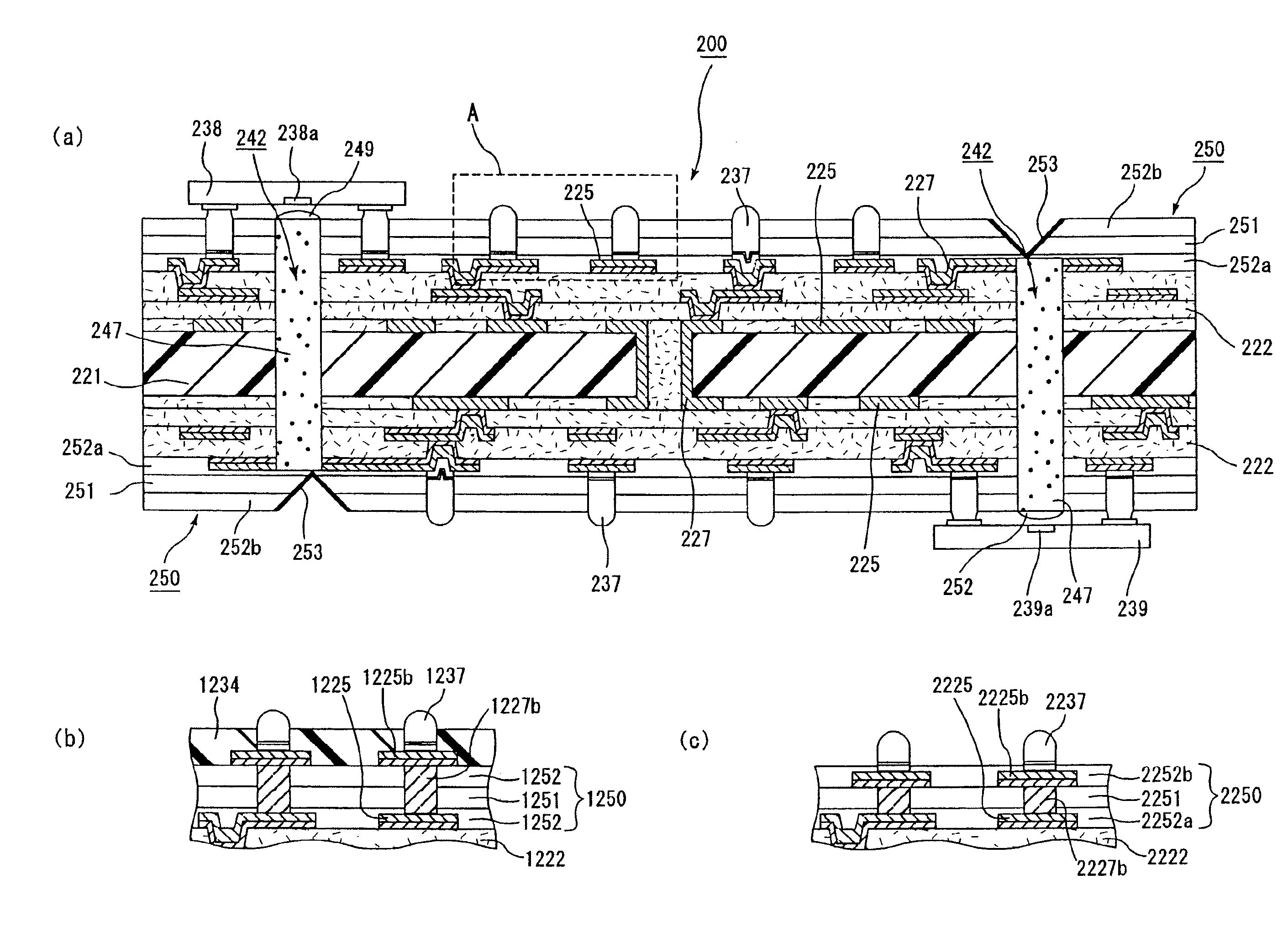
Multilayer printed circuit board
a printed circuit board and multi-layer technology, applied in the direction of circuit optical details, optical elements, instruments, etc., can solve the problems of less design freedom and increased size of printed circuit boards
- Summary
- Abstract
- Description
- Claims
- Application Information
AI Technical Summary
Problems solved by technology
Method used
Image
Examples
example 1
A. Manufacture of Resin Film for Insulating Layer
[0478]To 20 parts by weight of ethyldiglycol acetate and 20 parts by weight of solvent naphtha were added 30 parts by weight of bisphenol A-type epoxy resin (epoxy equivalent: 469, EPICOAT 1001 made by Yuka Shell Epoxy K.K.), 40 parts by weight of cresol novolak-type epoxy resin (epoxy equivalent: 215, EPICRON N-673 made by Dainippon Ink & Chemicals, Inc.) and 30 parts by weight of triazine structure-containing phenol novolak resin (phenolic hydroxide group equivalent: 120, PHENOLITE KA-7052 made by Dainippon Ink & Chemicals, Inc.) so as to be dissolved therein while being stirred under heat, and to this were further added 15 parts by weight of polybutadiene rubber with epoxidized terminals (DENAREX R-45EPT, made by Nagase Kasei Kogyo K.K.), 1.5 parts by weight of 2-phenyl-4,5-bis(hydroxymethyl) imidazole pulverized product, 2 parts by weight of fine pulverized silica and 0.5 parts by weight of silicone-based antifoamer, so that an ep...
example 2
1. Manufacture of Circuit Board A
[0521](1) A copper-clad multilayer board where copper foil of 18 μm was laminated on the two surfaces of an insulating substrate 10021 made of a glass epoxy resin or a BT (bismaleimide-triazine) resin having a thickness of 0.8 mm, and thus, surface conductor layers 10028 were formed, was used as a starting material (see FIG. 18(a)). First, holes were drilled in this copper-clad multilayer board and an electroless plating process was carried out, and in addition, holes 10009 were filled in with a resin composite 10030′, whereby conductor layers 10027′ which formed the wall surface of non-penetrating via holes were formed (see FIGS. 18(b) and 18(c)).
[0522]Here, as the resin composite, a resin composite gained by putting 100 parts by weight of a bisphenol F-type epoxy monomer (YL983U, made by Yuka Shell K.K., molecular weight: 310), 170 parts by weight of SiO2 particles in spherical form having an average particle diameter of 1.6 μm where the surface wa...
example 3
1. Manufacture of Circuit Board A
[0559](1) A circuit board A was manufactured in accordance with the same method as in Example 2.
2. Manufacture of Circuit Board B
[0560](2) A copper-clad multilayer board, where copper foil having a thickness of 18 μm was laminated on the two surfaces of an insulating substrate 10021 made of a glass epoxy resin or a BT (bismaleimide triazine) resin having a thickness of 0.8 mm so that surface conductor layers 10028 were formed, was used as a starting material (see FIG. 25(a)). First, holes were drilled in this copper-clad multilayer board, an electroless plating process was carried out, and holes 10009 were filled in with a resin composite, whereby conductor layers 10027′ which forms non-penetrating via holes on the wall surface thereof were formed (see FIGS. 25(b) and 25(c)).
[0561]Here, as the resin composite, the same resin composite as that used for the manufacture of circuit board A was used.
PUM
 Abstract
Description
Claims
Application Information
 - Generate Ideas
- Intellectual Property
- Life Sciences
- Materials
- Tech Scout
- Unparalleled Data Quality
- Higher Quality Content
- 60% Fewer Hallucinations
Browse by: Latest US Patents, China's latest patents, Technical Efficacy Thesaurus, Application Domain, Technology Topic, Popular Technical Reports.
© 2025 PatSnap. All rights reserved.Legal|Privacy policy|Modern Slavery Act Transparency Statement|Sitemap|About US| Contact US: help@patsnap.com


