Unlock instant, AI-driven research and patent intelligence for your innovation.

Pixel structure and method of fabricating the same

Active Publication Date: 2009-01-29
AU OPTRONICS CORP
View PDF13 Cites 4 Cited by
  • Summary
  • Abstract
  • Description
  • Claims
  • Application Information

AI Technical Summary

Benefits of technology

[0014]Specifically, the present invention discloses a method for fabricating pixel structures, in which a conductive layer composed of molybdenum, a dielectric layer composed of silicon oxide and an aluminum layer are deposited on a gate dielectric layer, and an isotropic etching process is performed to evenly remove a portion of the aluminum layer in both horizontal and vertical direction. Typically, the etchant utilized to etch aluminum material has the characteristic of achieving an isotropic etching process. Hence, when the aluminum layer is etched, not only the bottom portion of the aluminum layer is removed, the sidewall of the aluminum layer is also removed simultaneously to expose a required length for the lightly doped drain formed afterwards. In other words, the present invention could reduce the number of masks required to form the source / drain region from three to two, thereby reducing the overall cost of the fabrication process. According to an embodiment of the present invention, a stacked structure composed of silicon oxide and aluminum can also be formed on the capacitor electrode (such as the conductive layer composed of molybdenum) to increase the storage capacitance of the capacitor.

Problems solved by technology

It should be noted that the aforementioned process typically takes at least seven photomasks to complete the entire process for fabricating a pixel structure, which increases the overall cost of the fabrication significantly.
Despite the capacitor having such structure may qualify the demand for typical pixel structures, the capacity of these capacitors is still insufficient under many circumstances.

Method used


Image

  • Pixel structure and method of fabricating the same
  • Pixel structure and method of fabricating the same
  • Pixel structure and method of fabricating the same

Examples


Embodiment Construction

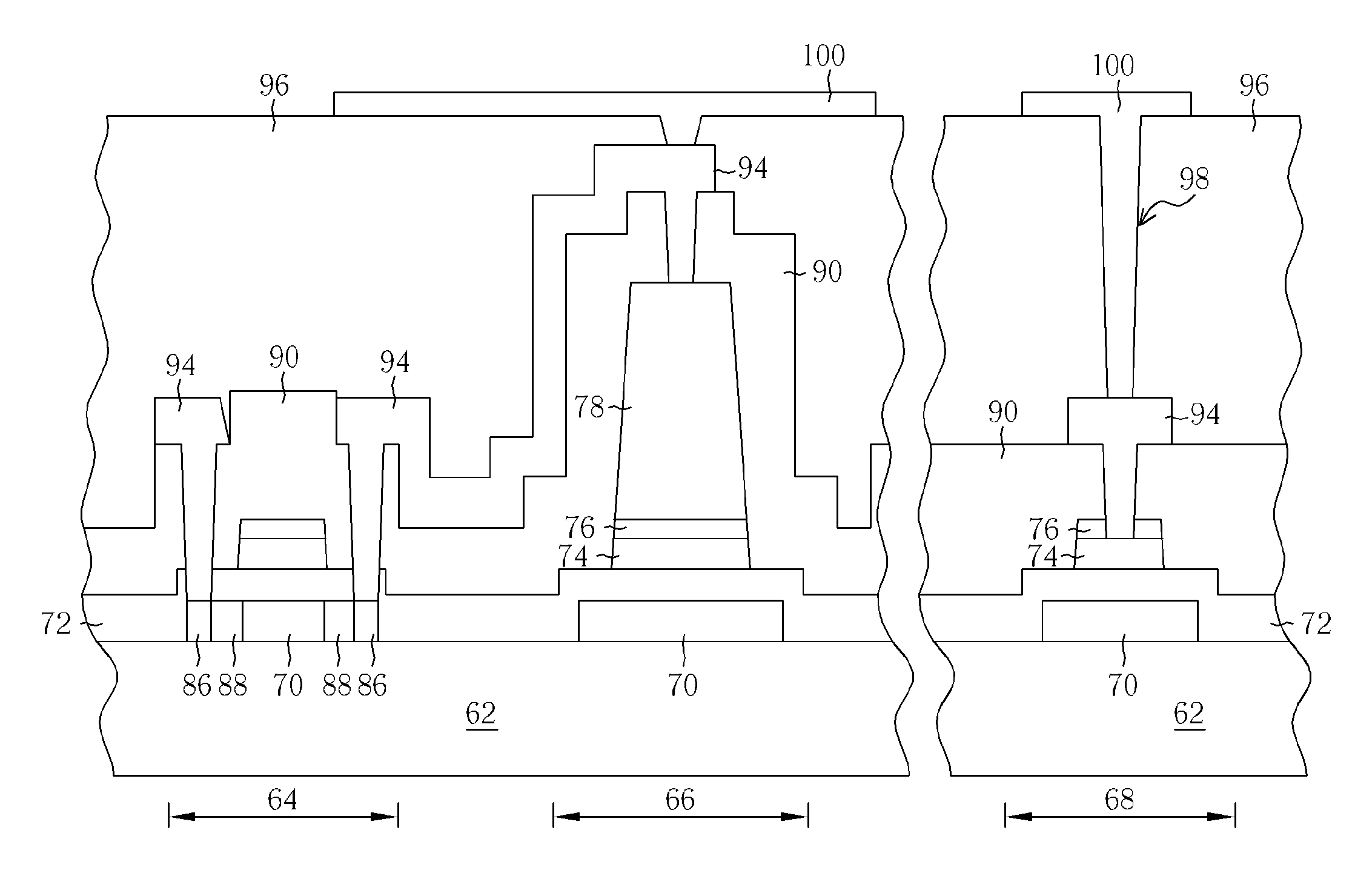
[0018]Referring to FIGS. 7-15, FIGS. 7-15 illustrate a method for fabricating a pixel structure according to a preferred embodiment of the present invention. As shown in FIG. 7, a substrate 62 is first provided. The substrate 62 can be a transparent glass substrate, in which the substrate 62 includes at least a transistor region 64, a capacitor region 66, and a pad region 68. A patterned semiconductor layer 70 is then formed on the transistor region 64, the capacitor region 66, and the pad region 68 of the substrate 62. The patterned semiconductor layer 70 disposed in the transistor region 64 is utilized to form a source / drain region of the transistor in the later process, and the patterned semiconductor layer 70 disposed in the capacitor region 66 is used to form a bottom capacitor electrode. The formation of the patterned semiconductor layer 70 can accomplished through a standard process for fabricating low temperature polysilicon semiconductors. For instance, an amorphous silicon...


PUM


Abstract

A method for fabricating pixel structures is disclosed. Specifically, the present invention deposits a conductive layer, a gate dielectric layer, and an aluminum layer on a gate dielectric layer, and performs an isotropic etching process to evenly etch a portion of the aluminum layer in the horizontal and vertical direction. By following this process, the number of photomasks used before the formation of the source / drain region can be reduced, and the conductive layer and the aluminum layer disposed on the capacitor electrode in the capacitor region can be used to increase the capacitance of the capacitor.

Description

BACKGROUND OF THE INVENTION[0001]1. Field of the Invention[0002]The invention relates a pixel structure and a method of fabricating the pixel structure.[0003]2. Description of the Prior Art[0004]A liquid crystal display (LCD) has gradually replaced a conventional cathode ray tube (CRT) display due to its small size, low radiation, and low power consumption. Generally speaking, an LCD panel includes an array substrate having thin film transistors thereon, a color filter substrate, and a liquid crystal layer disposed between the array substrate and the color filter substrate. The array substrate includes a plurality of pixel regions defined by a plurality of scan lines arranged in parallel, and a plurality of data lines arranged in parallel and perpendicular to the scan lines. Each pixel region is controlled by a thin film transistor as switch element and a pixel electrode to drive liquid crystal molecules to rotate in different extents for adjusting brightness outputs. The color filt...

Claims


Application Information

Patent Timeline
IPC IPC(8): H01L33/00H01L29/04H01L21/02
CPCG02F2001/136231H01L27/1288H01L27/1255H01L28/60G02F1/136231
Inventor CHIU, TA-WEICHENG, YI-SHENGYEN, SHIH-YI
Owner AU OPTRONICS CORP
Features
  • R&D
  • Intellectual Property
  • Life Sciences
  • Materials
  • Tech Scout
  • Unparalleled Data Quality
  • Higher Quality Content
  • 60% Fewer Hallucinations
Learn More