Method of Manufacturing Electromagnetic-Wave Shielding Plate, Electromagnetic-Wave Shielding Plate Manufactured Thereby, and Filter Display Using the Same

a technology of electromagnetic shielding plate and filter display, which is applied in the direction of identification means, instruments, cleaning using liquids, etc., can solve the problems of inability to meet the cost reduction demand of photolithography, disadvantageous factor of cost increase, and increasing the regulation of electromagnetic wave generated from electric products, so as to prevent the deterioration of image quality, and improve the effect of light-transmitting property

Inactive Publication Date: 2009-01-29
TORAY IND INC
View PDF7 Cites 35 Cited by
  • Summary
  • Abstract
  • Description
  • Claims
  • Application Information

AI Technical Summary

Benefits of technology

[0010]According to the present invention, since a resin layer is laminated on a metal layer, which is thin-line patterned on a transparent substrate, an electromagnetic-wave shielding plate superior in an electromagnetic-wave shielding property and a light-transmitting property and capable of preventing the deterioration of an image quality such as contrast and moire can be provided. Further, according to the present invention, the pattern of a resin layer 4 is formed on the metal layer 3 provided on one surface of the transparent substrate 1 (a) by a printing method (b), the metal layer 3 is etched by chemical etching (c), and a part 5 of the resin layer 4 protruding from the remaining metal layer 3 in a plate-surface direction is removed (d) when the electromagnetic-wave shielding plate is formed as shown in FIG. 1. Therefore, a thin-line mesh pattern including the metal layer and the resin layer can be formed by the printing method, which is a low-cost method. As a result, the electromagnetic-wave shielding plate superior in the non-visibility of the mesh pattern can be obtained. Further, the formation of the resin layer on the metal layer makes it difficult to damage the surface of the transparent substrate on which the metal layer is not formed during manufacture. In addition, when the electromagnetic-wave shielding plate is bonded to any other material, the substrate can be hardly damaged.

Problems solved by technology

In recent years, regulations imposed on an electromagnetic wave generated from an electric product have been increasingly strict due to radio disturbances inflicting various precision mechanical devices, measuring devices, and digital devices and adverse influences on human bodies.
On the other hand, it is necessary to use a copper foil whose one surface or both surfaces are subjected to black oxidation as the conductive metal layer in order to prevent the deterioration of an image quality such as contrast, and thus it is disadvantageously a factor for cost increase.
Further, the photolithography includes complicated long processes, and therefore the photolithography can not satisfy cost reduction demanded by the market.
This process, however, employs the photolithography after all, which also failed to satisfy the cost reduction demanded by the market.
However, in these printing methods, it is difficult to print a fine-pitch line width and to form a pattern with a thin-line of 20 μm or less, which is preferable in terms of the non-visibility of a mesh pattern.
Further, the electromagnetic-wave shielding plate thereby obtained is not satisfactory in terms of the light-transmitting property.

Method used


Image

  • Method of Manufacturing Electromagnetic-Wave Shielding Plate, Electromagnetic-Wave Shielding Plate Manufactured Thereby, and Filter Display Using the Same
  • Method of Manufacturing Electromagnetic-Wave Shielding Plate, Electromagnetic-Wave Shielding Plate Manufactured Thereby, and Filter Display Using the Same
  • Method of Manufacturing Electromagnetic-Wave Shielding Plate, Electromagnetic-Wave Shielding Plate Manufactured Thereby, and Filter Display Using the Same

Examples


example 1

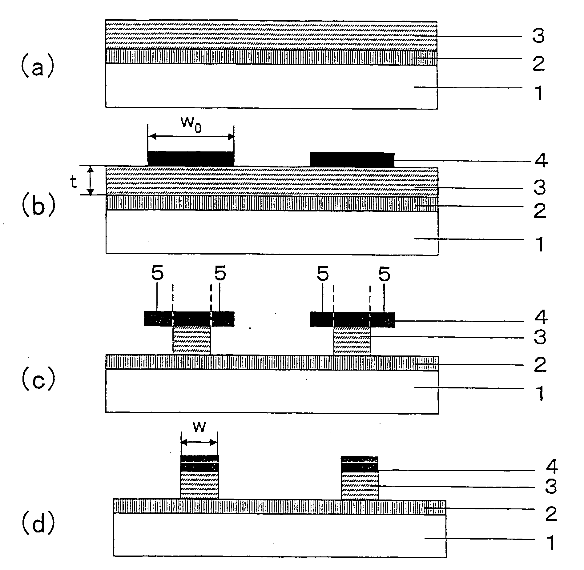
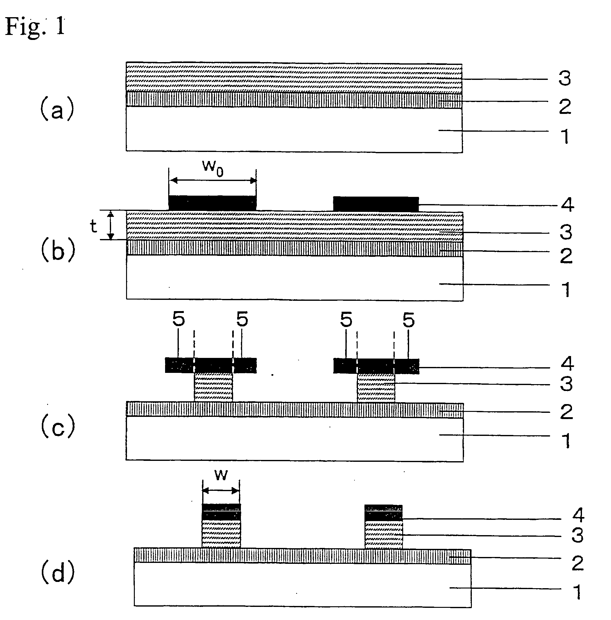
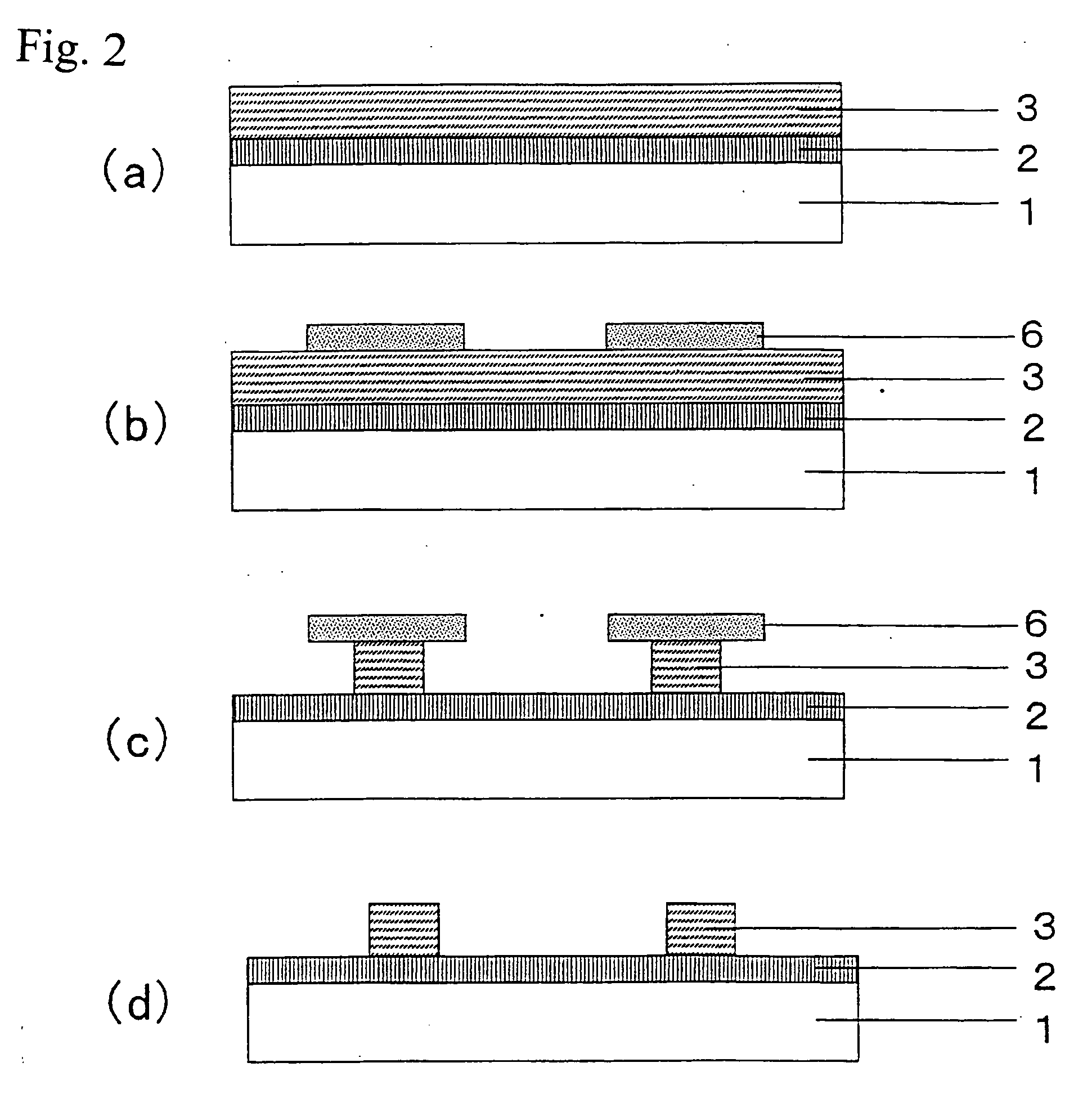
[0073]The copper foil having a thickness of 12 μm (manufactured by FURUKAWA CIRCUIT FOIL CO., LTD.) was laminated on the PET film having a total light transmittance of 93% and a thickness of 100 μm (manufactured by TORAY INDUSTRIES INC., “Lumirror” U34) as the metal layer via the two liquid type adhesive for a dry laminate (manufactured by Toyo-Morton, Ltd., base material AD-7P1 / curing agent CAT-10L) so that a conductive metallic plate was prepared. Next, the waterless plate (negative type TAN24E manufactured by TORAY INDUSTRIES INC.) and the ultraviolet-ray curing ink (manufactured by T&K TOKA COMPANY, “Best Cure” UV171, black ink) were used so that the grid-shape pattern having a line width of 35 μm and a line pitch of 250 μm was printed twice on the copper-foil surface of the conductive metallic plate by the offset printing method (speed 5 m / min.) and the plate was thereafter UV-cured. As a result, the black resin layer having a grid shape and a thickness of 3 μm was formed. Next...

example 2

[0076]Copper was sputtered and electrolytic-plated on the PET film having a total light transmittance of 89% and a thickness of 38 μm (manufactured by TORAY INDUSTRIES INC., “Lumirror” T60) as the metal layer so that the conductive metallic plate having a thickness of 5 μm was prepared. Next, the grid-shape pattern having a line width of 17 μm and a line pitch of 250 μm was printed once on the copper-plated surface of the conductive metallic plate in a manner similar to that of Example 1, and the plate was thereafter UV-cured. As a result, the black resin layer having a grid shape having a thickness of 1.5 μm was formed. Next, the plate was etched for 0.8 minute by the spray etching with the ferric chloride solution temperature-adjusted in the range of 35 to 40° C. so that the copper in the part where the resin layer was not printed and below the line-width end part of the resin layer was removed. Then, the plate was washed with water and dried. Then, the part of the black resin lay...

example 3

[0078]A conductive metallic plate was formed in a manner similar to Example 1 except that the PET film having a total light transmittance of 93% and a thickness of 125 μm was used in place of the PET film having a total light transmittance of 93% and a thickness of 100 μm, and the copper foil having a thickness of 10 μm (Nippon Denkai, Ltd.) was used in place of the copper foil having a thickness of 12 μm. On the copper-foil surface of the formed conductive metallic plate, the screen printing machine LS-150 manufactured by NEWLONG SEIMITSU KOGYO CO., LTD. and the two liquid type epoxy resin curing ink (manufactured by FUJIKURA KASEI CO., LTD., “Dotite” SH-3A) were used so that the lattice-shape pattern having a line width of 45 μm and the line pitch of 300 μm was printed once by the screen printing method (mesh #400, squeegee speed of 6 m / min., squeegee angle of 70 degrees), and heat was applied thereto at 120° C. for 30 minutes. As a result, the black resin layer having a grid shap...


PUM

PropertyMeasurementUnit
widthaaaaaaaaaa
widthaaaaaaaaaa
widthaaaaaaaaaa

Abstract

To provide an electromagnetic-wave shielding plate superior in an electromagnetic-wave shielding property, a light-transmitting property and non-visibility of a mesh pattern at low cost. A pattern of a resin layer is printed on a metal layer of a transparent substrate by a printing method. After that, the metal layer is over-etched with the resin layer used as an etching mask, and a part of the resin layer protruding from the remaining metal layer in a plate-surface direction is removed. As a result, an electromagnetic-wave shielding plate superior in an electromagnetic-wave shielding property and non-visibility and having, for example, a pattern line width of 3 μm or more and 25 μm or less.

Description

FIELD OF THE INVENTION[0001]The present invention relates to an electromagnetic-wave shielding plate transparently visible and used for an image display unit, or the like, which generates an electromagnetic wave, such as a plasma display panel (PDP) and a cathode ray tube (CRT), a method of manufacturing the electromagnetic-wave shielding plate, and a filter and a display in which the electromagnetic-wave shielding plate is used.BACKGROUND OF THE INVENTION[0002]In recent years, regulations imposed on an electromagnetic wave generated from an electric product have been increasingly strict due to radio disturbances inflicting various precision mechanical devices, measuring devices, and digital devices and adverse influences on human bodies. Therefore, the emission of an electromagnetic wave has been legally controlled, for example, by the VCCI (Voluntary Control Council for Interference by data processing equipment electronic office machine). In a PDP which emits a particularly strong...

Claims


Application Information

Patent Timeline
Patent Type & Authority Applications(United States)
IPC IPC(8): B32B3/10B44C1/22
CPCH05K9/0096Y10T428/24917B32B15/08G09F9/00
Inventor WATANABE, OSAMUYOSHIOKA, TADASHIGOTO, KAZUKIUEBA, TAKAYOSHI
Owner TORAY IND INC
Why Eureka
Try Eureka