
Endpoint Detection Device For Realizing Real-Time Control Of Plasma Reactor, Plasma Reactor With Endpoint Detection Device, And Endpoint Detection Method

Inactive Publication Date: 2009-01-29
DMS CO LTD
View PDF9 Cites 16 Cited by
  • Summary
  • Abstract
  • Description
  • Claims
  • Application Information

AI Technical Summary

Benefits of technology

[0013]An aspect of exemplary embodiments of the present invention is to address at least the problems and / or disadvantages and to provide at least the advantages described below. Accordingly, an aspect of exemplary embodiments of the present invention is to provide an endpoint detection device for, with execution of a real-time process wafer etch or deposition process, computing OES data generated in real time and loading vectors previously calculated in a previous etch or deposition process, and generating a product value for determining an etch or deposition endpoint, thereby detecting an endpoint without real-time normalization of the OES data, increasing a detection speed, and realizing a real-time control of a plasma reactor.
[0014]Another aspect of exemplary embodiments of the present invention is to provide a plasma reactor comprising the endpoint detection device for, with execution of a real-time process wafer etch or deposition process, computing OES data generated in real time and loading vectors previously calculated during a previous etch or deposition process, and generating a product value for determining an etch or deposition endpoint, thereby detecting an endpoint without real-time normalization of the OES data, increasing a detection speed, and realizing a real-time control of a plasma reactor.
[0015]A further another aspect of exemplary embodiments of the present invention is to provide an endpoint detection method for, with execution of a real-time process wafer etch or deposition process, computing OES data generated in real time and loading vectors previously calculated during a previous etch or deposition process, and generating a product value for determining an etch or deposition endpoint, thereby detecting an endpoint without real-time normalization of the OES data, increasing a detection speed, and realizing a real-time control of a plasma reactor.

Problems solved by technology

Accordingly, abnormal process errors of the semiconductor processing equipments become major obstacles to obtain a good quality of semiconductor product as well as cause economic loss and time loss.
However, a wavelength of lights generated by etched materials is distributed over several frequency bands and therefore, it is very difficult to select one wavelength of most significance serving as a criterion for determining an etch endpoint.
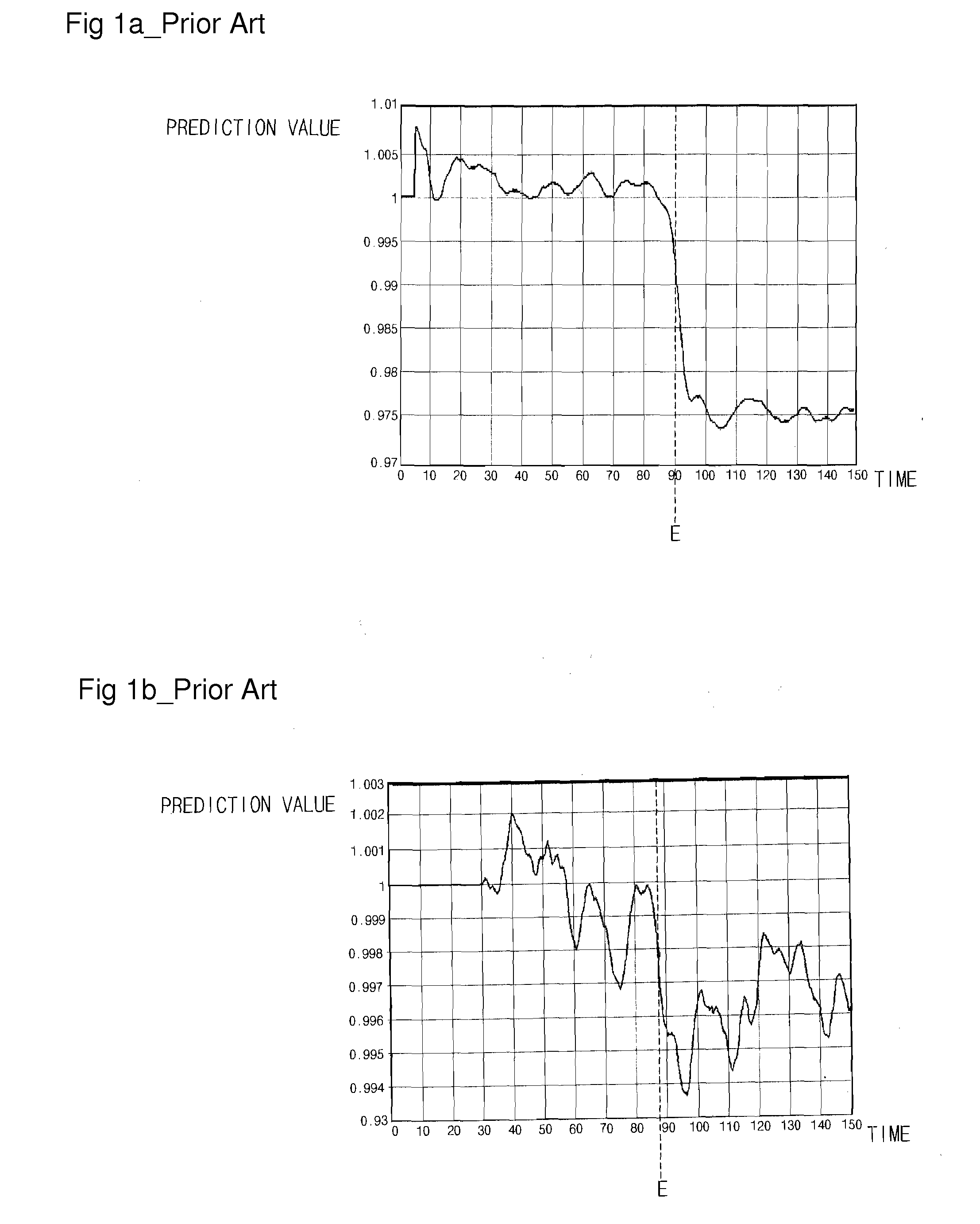
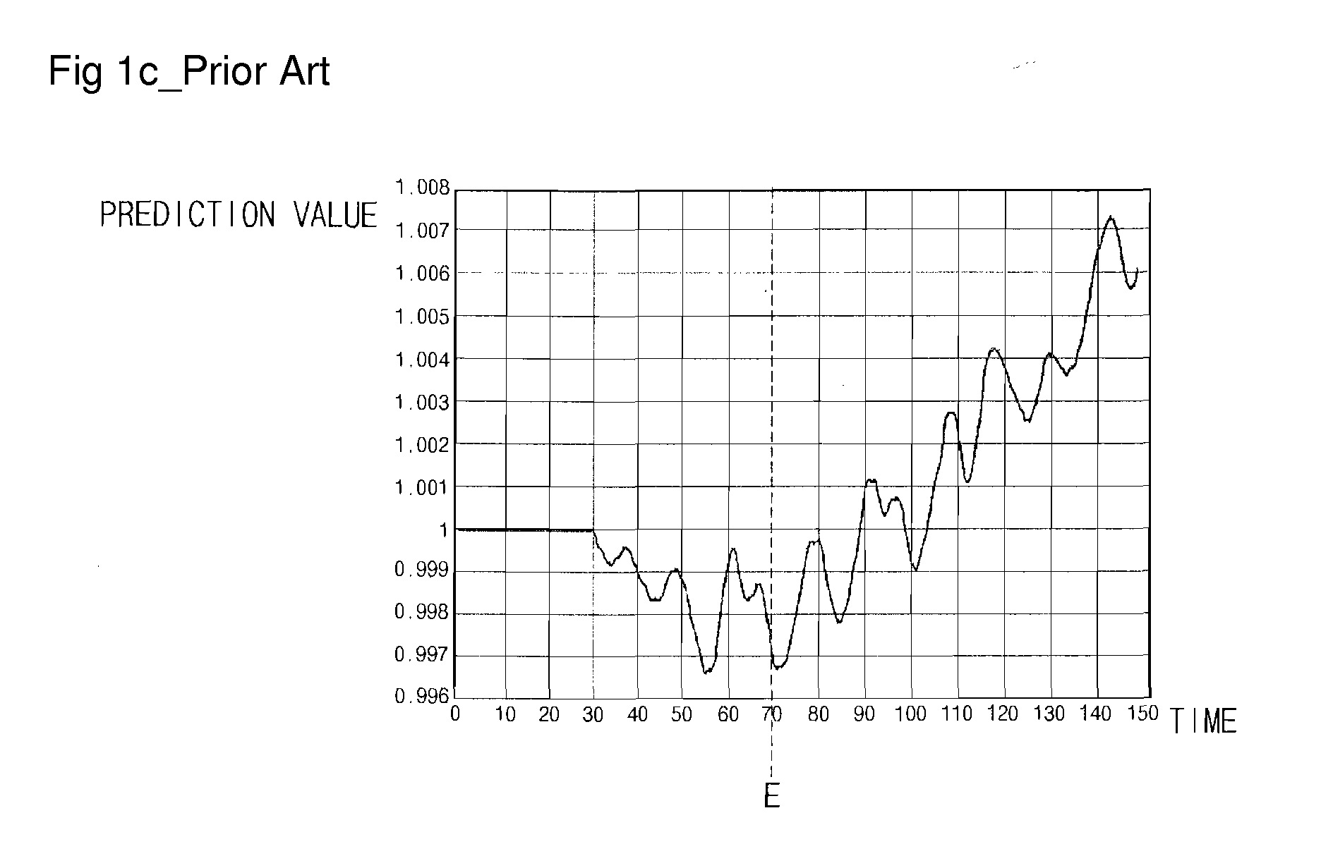
However, in a conventional endpoint detection method using PCA, a detection speed is very slow because it actually takes a long time to real-time normalize voltage level signals (that is, Optical Emission Spectrometer (OES) data).
In conclusion, PCA is almost impossible to real-time determine an in-chamber status quickly and thereby the plasma reaction controller is impossible to real-time control reaction conditions within a plasma reaction chamber as well.
This problem becomes more serious because of the recent development of sensors to have as better operation performance as the sensors receive light signals of thousands of wavelengths at several times even for one second.
That is, the sensors can receive a large amount of light signals with the improvement of operation performance of the sensors; however, it takes a very long time to store and normalize voltage level data corresponding to the large amount of received light signals.
Accordingly, an endpoint detection speed gets slower and resultantly, it is impossible to control plasma reaction conditions in real time.

Method used


Image

  • Endpoint Detection Device For Realizing Real-Time Control Of Plasma Reactor, Plasma Reactor With Endpoint Detection Device, And Endpoint Detection Method
  • Endpoint Detection Device For Realizing Real-Time Control Of Plasma Reactor, Plasma Reactor With Endpoint Detection Device, And Endpoint Detection Method
  • Endpoint Detection Device For Realizing Real-Time Control Of Plasma Reactor, Plasma Reactor With Endpoint Detection Device, And Endpoint Detection Method

Examples


Embodiment Construction

[0043]Exemplary embodiments of the present invention will now be described in detail with reference to the annexed drawings. In the following description, a detailed description of known functions and configurations incorporated herein has been omitted for conciseness.

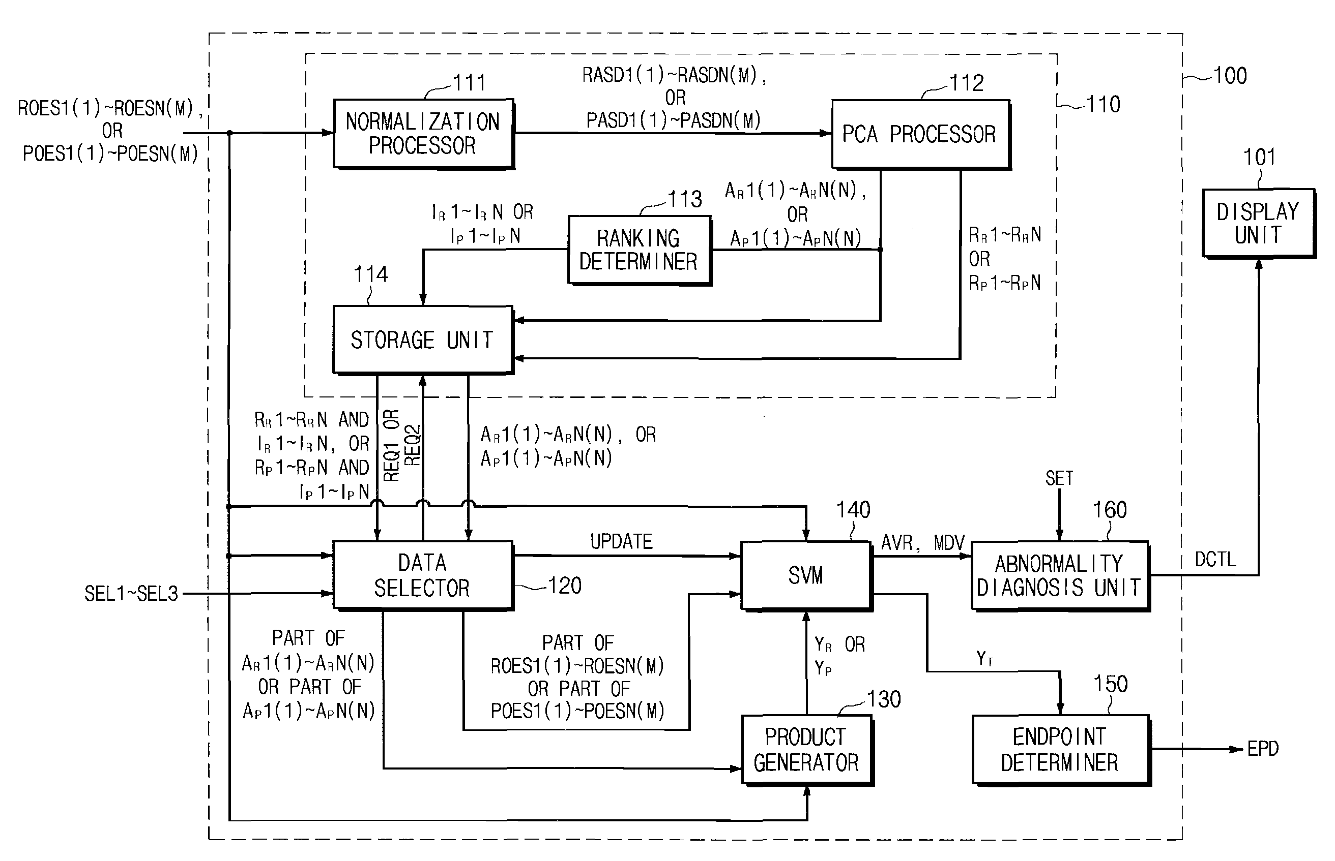
[0044]FIG. 2 is a block diagram illustrating an endpoint detection device according to an exemplary embodiment of the present invention.

[0045]Referring to FIG. 2, the endpoint detection device 100 includes an OES data operation unit 110, a data selector 120, a product generator 130, an SVM 140, an endpoint determiner 150, and an abnormality diagnosis unit 160. The OES data operation unit 110 includes a normalization processor 111, a PCA processor 112, a ranking determiner 113, and a storage unit 114.

[0046]During a reference wafer etch or deposition process, the normalization processor 111 normalizes reference OES data (ROES1(1) to ROESN(M)) (N, M: integers) and outputs reference average scaling data (RASD1(1) to RASDN(...


PUM

PropertyMeasurementUnit
Timeaaaaaaaaaa
Wavelengthaaaaaaaaaa

Abstract

An endpoint detection device, a plasma reactor with the endpoint detection device, and an endpoint detection method are provided. The endpoint detection device includes an OES data operation unit, a data selector, a product generator, an SVM, and an endpoint determiner. The OES data operation unit processes reference OES data by normalization and PCA. The data selector selects part of the linear reference loading vectors and selects part of the selected linear reference loading vectors. The product generator outputs at least one reference product value. The SVM performs regression and outputs a prediction product value. The endpoint determiner detects a process wafer etch or deposition endpoint and outputs a detection signal.

Description

BACKGROUND OF THE INVENTION[0001]1. Field of the Invention[0002]The present invention relates to a device used in a semiconductor manufacturing process. More particularly, the present invention relates to an endpoint detection device for detecting an etch endpoint or a deposition endpoint during a semiconductor etch or deposition process, a plasma reactor with the endpoint detection device, and an endpoint detection method.[0003]2. Description of the Related Art[0004]In general, until to finish one semiconductor product from a wafer, a series of very complex semiconductor processes are required. A variety of semiconductor processing equipments each are used in a series of semiconductor processes. Operation performance (that is, process conditions) of the semiconductor processing equipments each is a factor of determining operation performance of finished semiconductor products. Accordingly, abnormal process errors of the semiconductor processing equipments become major obstacles to ...

Claims


Application Information

Patent Timeline
IPC IPC(8): H01L21/3065B05C11/00H01L21/00
CPCG01N21/71H01J37/32935H01L21/67253H01L21/67069H01J37/32963H01L21/02
Inventor PARK, KUN JOOHAN, KWANG HOONKIM, KEE HYUNLEE, WEON MOOKHAN, KYOUNGHOONCHAE, HEEYEOP
Owner DMS CO LTD
Learn More