Method for manufacturing semiconductor device

Inactive Publication Date: 2009-01-29
SEMICON ENERGY LAB CO LTD
View PDF17 Cites 5 Cited by
  • Summary
  • Abstract
  • Description
  • Claims
  • Application Information

AI Technical Summary

Benefits of technology

[0019]The thickness of the amorphous semiconductor film is preferably about equal to or greater than the height of the projection portion. Accordingly, defective formation of the semiconductor film can be prevented.
[0020]According to the method for manufacturing a semiconductor device of the invention, the amorphous semiconductor film is deposited over the projection portion and the depression portions adjacent to the projection portion, which are formed over the insulating substrate. The amorphous semiconductor film is irradiated with laser light to be crystallized and melted so that the surface of the cry

Problems solved by technology

In addition, plasma etching may cause characteristic deterioration such as damage to the upper part of the semiconductor layer, transformation into an amorphous state, and increase in r

Method used


Image

  • Method for manufacturing semiconductor device
  • Method for manufacturing semiconductor device
  • Method for manufacturing semiconductor device

Examples


Example

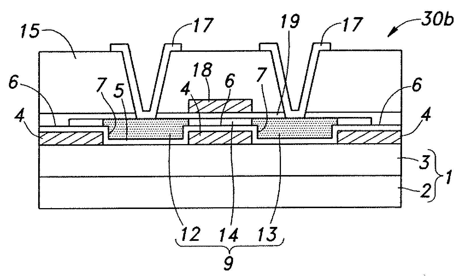
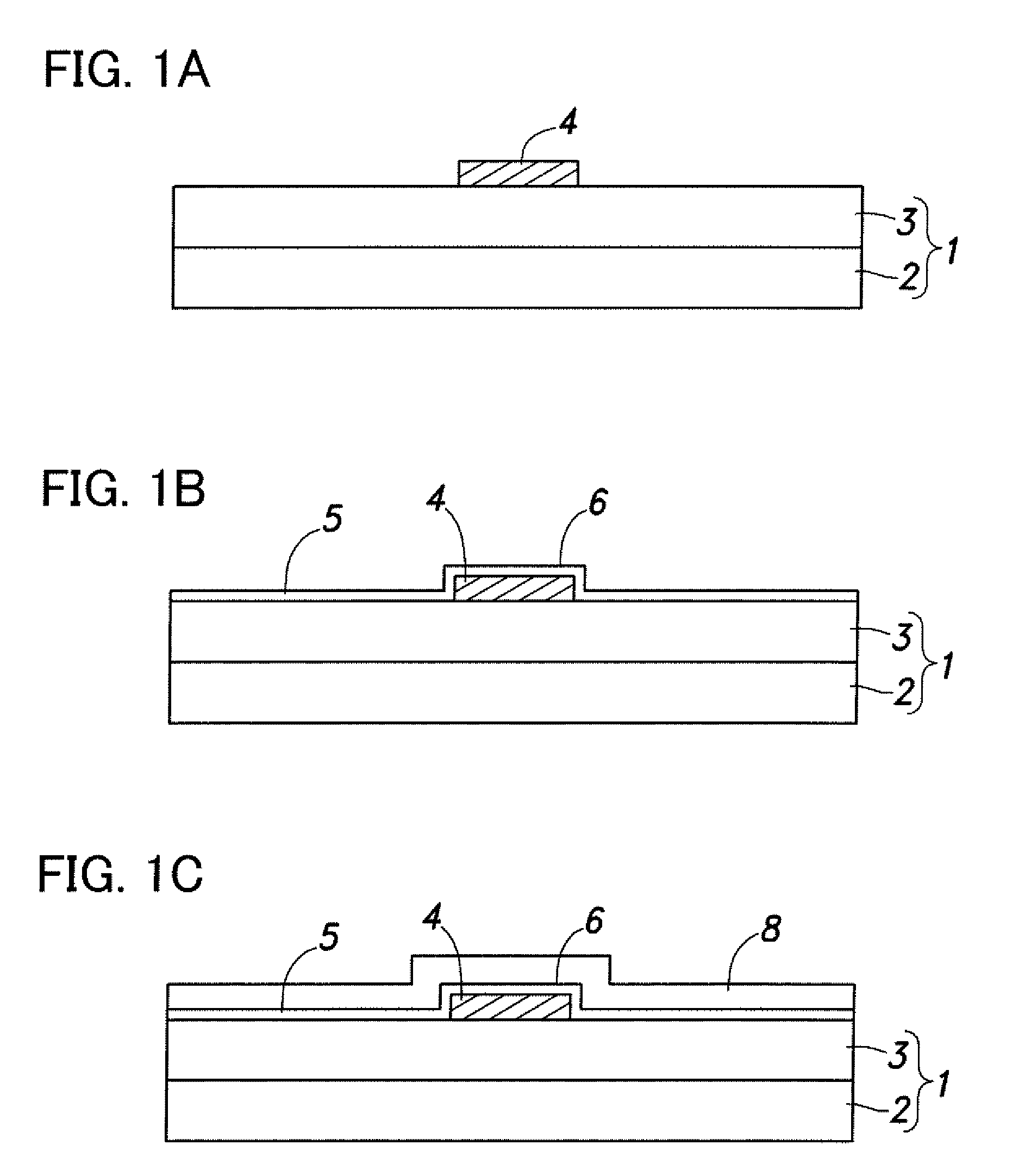
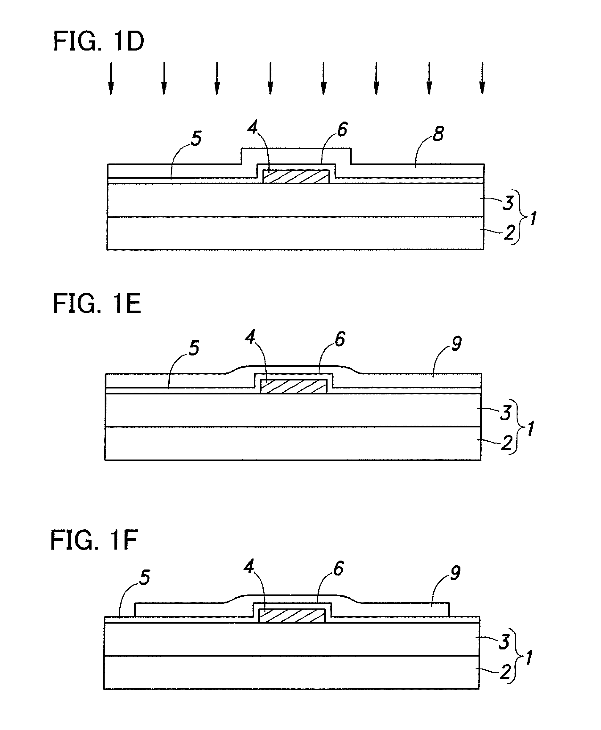
[0030]FIGS. 1A to 1J are cross-sectional views illustrating a method for manufacturing a semiconductor device (TFT) according to a preferred embodiment of the invention.

[0031]As illustrated in FIG. 1A, a conductive film is deposited over an insulating substrate 1 having an insulating surface, and patterned by etching or the like to form an island-like conductive film 4. In this example, the insulating substrate 1 includes a substrate 2 with a flat surface and a base film 3 formed over the substrate 2. The island-like conductive film 4 extends in a direction perpendicular to the paper of the drawing to be connected to a gate wiring.

[0032]The substrate 2 with a flat surface may be, for example, a glass substrate, a quartz substrate, a single crystal silicon substrate, a metal substrate, a heat-resistant plastic substrate, or the like. The insulating substrate 1 is only required to have an insulating surface so that a semiconductor film can be deposited thereover in a subsequent step, ...


PUM


Abstract

A method for manufacturing a semiconductor device, by which a bottom gate thin film transistor that has an improved S value and a channel forming region with a smaller thickness than that of a source region and a drain region can be manufactured in a simple process. An island-like conductive film is formed over a surface of an insulating substrate in a portion corresponding to a channel forming region, and is covered with an insulating film to form a projection portion. After an amorphous semiconductor film is deposited to cover the projection portion, the amorphous semiconductor film is irradiated with laser light so as to be melted and crystallized. Part of the melted semiconductor over the projection portion flows into regions adjacent to both sides of the projection portion, which results in reduction in thickness of the semiconductor film over the projection portion (channel forming region).

Description

BACKGROUND OF THE INVENTION[0001]1. Field of the Invention[0002]The present invention relates to a method for manufacturing a semiconductor device. In particular, the invention relates to a method for manufacturing a bottom gate thin film transistor that includes a channel forming region having a thickness smaller than that of a source region and a drain region.[0003]2. Description of the Related Art[0004]It is known that in a thin film transistor (hereinafter referred to as a TFT), the S value that indicates the switching characteristics (subthreshold characteristics) of a transistor can be improved (i.e., reduced) by reducing the thickness of a channel forming region. The S value here is a gate voltage (potential difference between a source region and a gate electrode based on the potential of the source region) that is required to increase a current between the source region and a drain region (subthreshold current) by one digit. When the S value decreases, the slope of the subth...

Claims


Application Information

Patent Timeline
IPC IPC(8): H01L21/336
CPCH01L29/66765
Inventor YOKOI, TOMOKAZUISOBE, ATSUOKURATA, MOTOMUSHICHI, TAKESHIOHGARANE, DAISUKESHINGU, TAKASHI
Owner SEMICON ENERGY LAB CO LTD
Why Eureka
Try Eureka