Back contact solar cell

Inactive Publication Date: 2015-05-14
NEO SOLAR POWER CORP
View PDF4 Cites 1 Cited by
  • Summary
  • Abstract
  • Description
  • Claims
  • Application Information

AI Technical Summary

Benefits of technology

[0011]As mentioned, in comparison with the back contact solar cell of prior art, which has the p-n junction formed in the conductive silicon substrate and adopts the intrinsic layer merely as a passivation layer. A second conductive type semiconductor layer is formed on the intrinsic layer, therefore, the substrate body with the first conductive type semiconductor material, the intrinsic layer and the second conductive type semiconductor layer f

Problems solved by technology

In addition, the problem is that too many defects formed in the interfaces between the first conductive type sil

Method used


Image

  • Back contact solar cell
  • Back contact solar cell
  • Back contact solar cell

Examples


Example

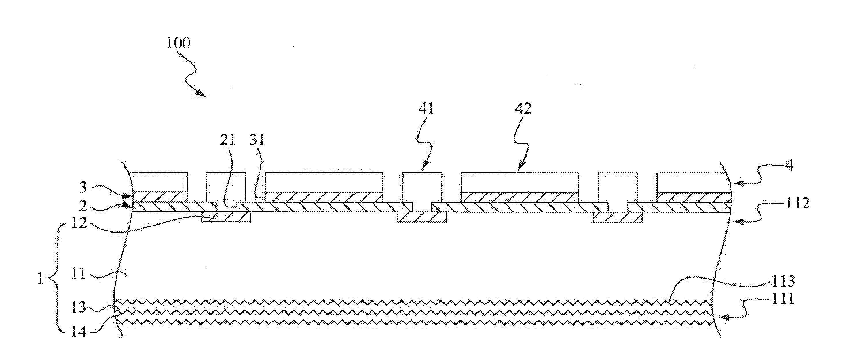
[0031]FIG. 3 is a cross-section view showing a back contact solar cell in accordance with a first preferred embodiment of the present invention.

[0032]As shown, the back contact solar cell 100 includes a solar cell substrate 1, an intrinsic layer 2, a second conductive type semiconductor layer 3, and an electrode layer 4.

[0033]The solar cell substrate 1 includes a substrate body 11, a plurality of first conductive type semiconductor doped regions 12, a front surface field layer 13, and an anti-reflection layer 14.

[0034]The substrate body 11 has a front side 111, a back side 112, and a textured surface 113. The back side 112 is opposite to the front side 111. The textured surface 113 is formed on the front side 111. The substrate body 11 may be a silicon substrate, which is doped with a first conductive type semiconductor of a first doping concentration. The first conductive type semiconductor is the P-type semiconductor selected from the IIA group or IIIA group elements on the period...


PUM


Abstract

A back contact solar cell includes a solar cell substrate, an intrinsic layer, a second conductive type semiconductor layer and an electrode layer. The solar cell substrate includes a substrate body doped with a first conductive type semiconductor and a plurality of first conductive type semiconductor doped regions. The first conductive type semiconductor doped region is formed on a back side of the substrate body. The intrinsic layer is formed on the back side, and includes a plurality of first openings to expose the first conductive type semiconductor doped regions. The second conductive type semiconductor layer is deposited on the intrinsic layer, and includes a plurality of second openings correspond the first openings. The electrode layer includes a plurality of first electrode regions and a second electrode region. The first electrode regions are disposed on the first conductive type semiconductor doped regions. The second electrode regions are disposed on the second conductive type semiconductor layer, and separated with the first electrode regions.

Description

FIELD OF THE INVENTION[0001]The present invention relates to a back contact solar cell, and more particularly relates to a back contact solar cell having an intrinsic layer and a second conductive type semiconductor layer deposited on a substrate body doped with a first conductive type semiconductor material.BACKGROUND OF THE INVENTION[0002]Due to the supply issue of oil and the greenhouse gas emission, solar cell development has accelerated because solar energy is the sustainable energy. The most common solar cell includes a silicon wafer doped with P-type semiconductor and N-type semiconductor to form the PN junction. When the solar cell is illuminated by sunlight to generate electron-hole pairs, the electric field created on the PN junction promotes charge flow to separate the electrons and holes, which are further directed by the external circuitry connected to the electrodes.[0003]However, the solar cells in present usually have the two electrodes located on the front surface a...

Claims


Application Information

Patent Timeline
IPC IPC(8): H01L31/075H01L31/065H01L31/0224
CPCH01L31/075H01L31/065H01L31/022441H01L31/0352H01L31/0747H01L31/1804Y02E10/547Y02E10/548Y02P70/50
Inventor HUANG, CHORNGJYEYANG, FENG-YUPEI, SHAN-CHUANGYEH, CHING-CHUNCHUANG, TIEN-SHAO
Owner NEO SOLAR POWER CORP
Why Eureka
Try Eureka