Thin film piezoelectric resonator and method of manufacturing the same

a piezoelectric resonator and thin film technology, applied in the field of wireless communication, can solve the problems of difficult to constitute the rf front end, difficult to be difficult to be downsized and thinned to several millimeters, so as to improve the resonating performance

Active Publication Date: 2009-02-05
KK TOSHIBA
View PDF12 Cites 93 Cited by
  • Summary
  • Abstract
  • Description
  • Claims
  • Application Information

AI Technical Summary

Benefits of technology

[0013]The invention is aimed at providing a thin film piezoelectric resonator which can overcome the foregoing problems of the related art, improve resonating performance thereof, and be miniaturized.

Problems solved by technology

It is technically difficult to constitute the RF front end only by an LSI chip because the RF front end has a very complicated structure.
The filters can filter high frequency signals using passband characteristics of a cavity resonator or an LC circuit, and is essentially difficult to be downsized and to be thinned to several millimeters or less.
In other words, communication devices operating on high frequency bands have limitations on their miniaturization.
Especially, a general purpose filter can be easily made as thin as 1 mm or less, which is usually very difficult.
However, there are the following new problems when a high frequency module is made using the thin film piezoelectric resonator on which a transistor, IC, LSI and so on are mounted.
This phenomenon extensively deteriorates resonance performance of the thin film piezoelectric resonator, or makes the resonance performance variable.
However, since such an upper electrode 104 becomes large, it is impossible to miniaturize a filter including thin film piezoelectric resonators.
This not only increases the number of manufacturing processes but also reduces an yield of the thin film piezoelectric resonator 100.
However, a sufficient processing margin cannot be secured.

Method used


Image

  • Thin film piezoelectric resonator and method of manufacturing the same
  • Thin film piezoelectric resonator and method of manufacturing the same
  • Thin film piezoelectric resonator and method of manufacturing the same

Examples


first embodiment

[Configuration of Thin Film Piezoelectric Resonator]

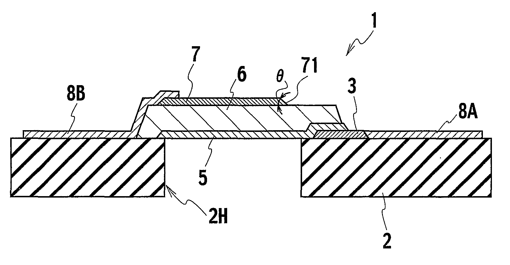
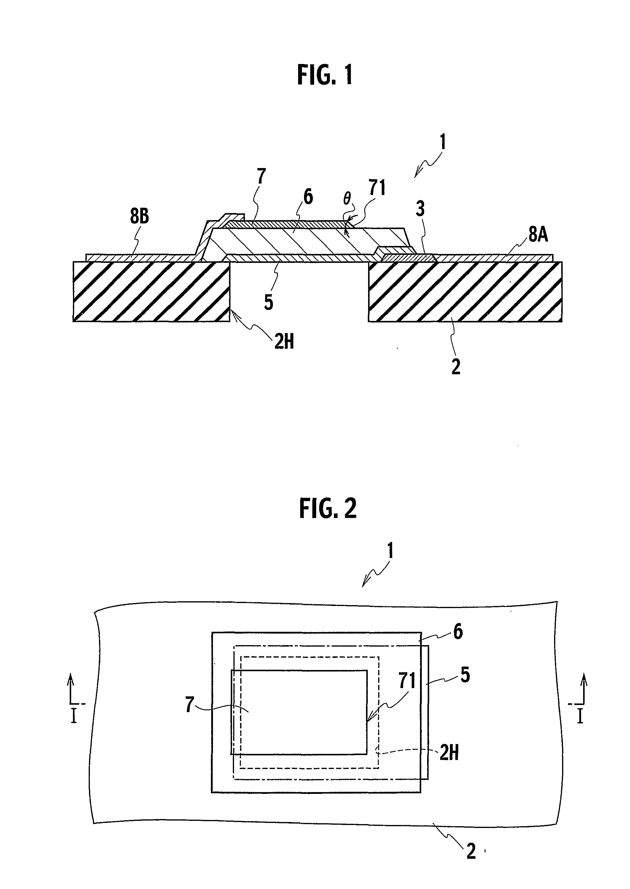
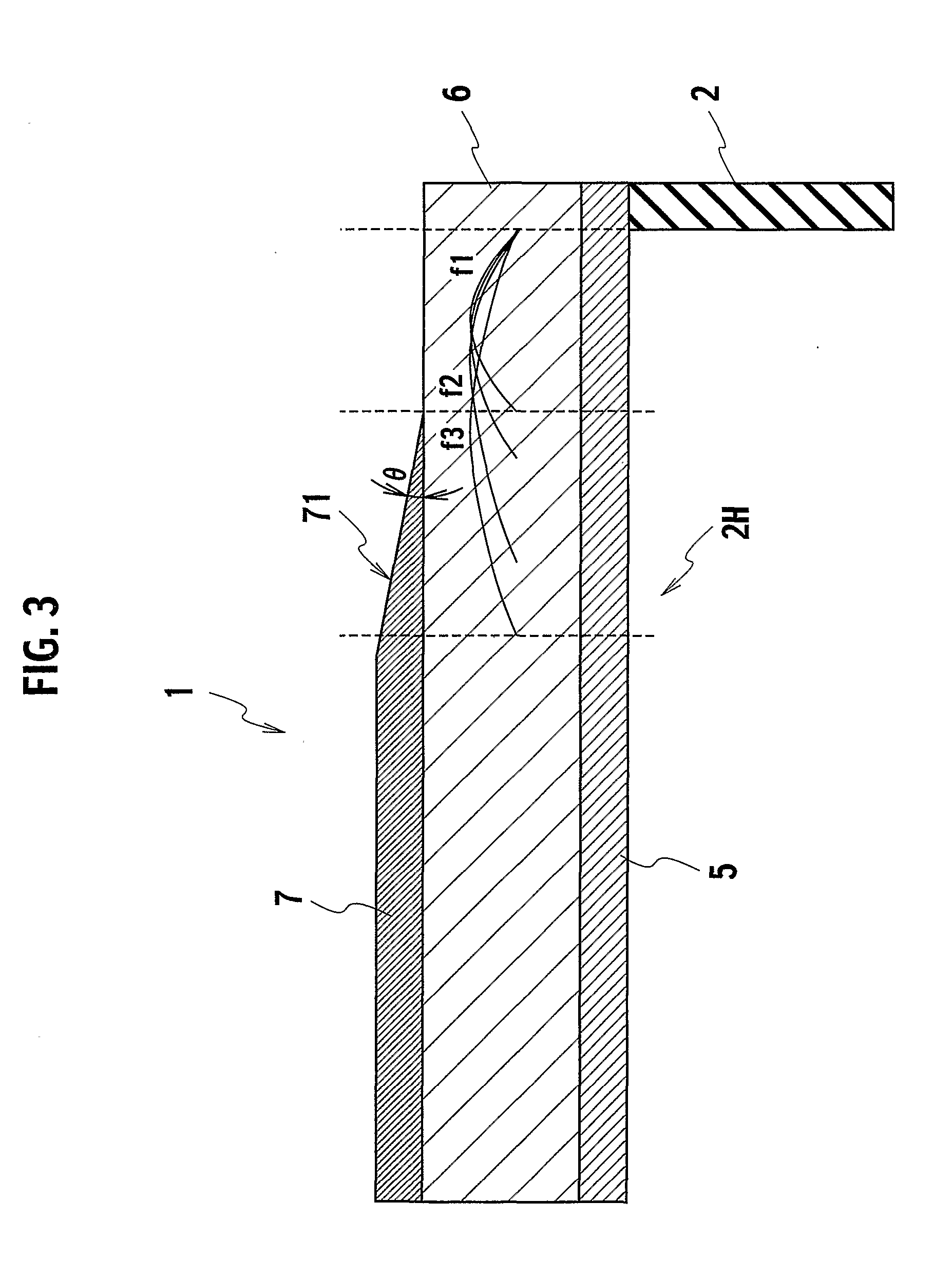
[0037]Referring to FIG. 1 to FIG. 3, a thin film piezoelectric resonator 1 (called the “piezoelectric resonator 1”) in this embodiment includes a substrate 2 having a cavity 2H; a first electrode (lower electrode) 5 extending over the cavity 2H; a piezoelectric film 6 extending on first electrode 5; and a second electrode 7 extending partly on the piezoelectric film 6. A periphery 71 of the second electrode 7 overlaps on the cavity 2H, and is tapered to have an inner angle θ of 30 degrees or smaller defined by a part of the periphery thereof and a bottom thereof, e.g., the inner angle θ is set between 15 degrees and 30 degrees in the first embodiment.

[0038]The substrate 2 is made of silicon in this embodiment. The cavity 2H is in the shape of a rectangle, for example. When an acoustic reflector is used, it is placed in the cavity 2H, which is made by digging a part of the substrate 2.

[0039]The first electrode 5 extends over the cav...

example

[0058]A specific example of the piezoelectric resonator 1 of the first embodiment will be described with reference to FIG. 1 to FIG. 3.

[0059]In the piezoelectric resonator 1, the first electrode 5 has a dual structure in which the lower part thereof is amorphous in order to improve the orientation of the piezoelectric film 6, i.e., AlN. Resonance characteristics can be improved by controlling the orientation of AlN. The orientation of the sputtered AlN film is controlled to be 1.5 degrees or less with respect to the rocking curve of X rays. Further, the stress of AlN is also controlled in order to stabilize the components bridging the cavity 2H. Specifically, the substrate 2 is subject to the high speed RIE from its rear surface in order to make the cavity 2H. The first and second wirings 8A and 8B are made of gold (Au) or Al.

[0060]The piezoelectric resonator 1 operates on a 2 GHz band, has an electrical-mechanical coupling constant of 6.7%, and a resonance Q value of 800. During th...

second embodiment

[0063]A second embodiment is intended to promote the suppression of the spurious vibrations in the piezoelectric resonator of the first embodiment, and to provide a piezoelectric resonator which is reliable for a long period of time.

[0064]Referring to FIG. 10, the piezoelectric resonator 1 of this embodiment includes an insulator (passivation film) 9 which has a dielectric constant different from that of the second electrode 7, and uniform thickness. The insulator 9 extends over the second electrode 7 including the edge 71, and the piezoelectric film 6. In short, the insulator 9 is in direct contact with the second electrode 7. The insulator 9 is preferably made of a silicon-nitride film (Si3N4) which is prepared by the CVD process and is approximately 2 nm to 50 nm thick. Alternatively, the insulator 9 may be made of a silicon-oxide film (SiO2), an AlN film and so on which have dielectric constants different from that of the second electrode 7. Further, the insulator 9 may be prepa...


PUM

PropertyMeasurementUnit
inner angleaaaaaaaaaa
thickaaaaaaaaaa

Abstract

A thin film piezoelectric resonator includes a substrate having a cavity; a first electrode extending over the cavity; a piezoelectric film placed on the first electrode; and a second electrode placed on the piezoelectric film, the second electrode having a periphery partially overlapping on the cavity and tapered to have an inner angle of 30 degrees or smaller defined by a part of the periphery thereof and a bottom thereof.

Description

TECHNICAL FILED[0001]This invention relates to a thin film piezoelectric resonator and a method of manufacturing the same, and more particularly relates to a thin film piezoelectric resonator which uses axial vibrations in a direction of the thickness of a thin piezoelectric film, and the method of manufacturing such a thin film piezoelectric resonator.BACKGROUND ART[0002]Along with a remarkable breakthrough in the field of wireless communications, a variety of developments have been in progress in order to accelerate information transmission. With the wireless communications, frequency bands of approximately 2 GHz are in wide use in order to cope with the introduction of PHS systems, third generation cellular phones, wireless LAN, and so on. Further, the number of users and wireless terminals are extensively increased. The higher the information transmission speeds, the higher the carrier frequencies. Wireless LAN systems operating on a 5 GHz frequency band are now in business use....

Claims


Application Information

Patent Timeline
Patent Type & Authority Applications(United States)
IPC IPC(8): H01L41/047H01L41/22H03H3/02H03H9/17
CPCH03H3/02H03H9/02118Y10T29/42H03H9/132H03H9/174H03H9/13H03H9/24
Inventor ITAYA, KAZUHIKOOHARA, RYOICHISANO, KENYAYASUMOTO, TAKAAKIYANASE, NAOKO
Owner KK TOSHIBA
Why Eureka
Try Eureka