Substrate processing apparatus, heating apparatus for use in the same, method of manufacturing semiconductors with those apparatuses, and heating element supporting structure

a technology of heating apparatus and processing apparatus, which is applied in the direction of lighting and heating apparatus, oven heating elements, baking ovens, etc., can solve the problems of thermal deformation of heating members at the center region, relative displacement of along the circumference to each other not being regulated, etc., to achieve superior effects, improve heat radiation, and reduce physical strength

Active Publication Date: 2009-02-05
KOKUSA ELECTRIC CO LTD +1
View PDF3 Cites 16 Cited by
  • Summary
  • Abstract
  • Description
  • Claims
  • Application Information

AI Technical Summary

Problems solved by technology

However in the conventional heating module described above, in structure of the supporting pieces, the relative displacement of along the circumference to each other is not regulated.
Moreover, as the heating wire repeats its expanding and shrinking action, it will move together with the supporting pieces radially of the vertical furnace or be deformed irregularly due to its thermal distortion.
However, the heating member fails to be protected from being thermally deformed at its center region.

Method used


Image

  • Substrate processing apparatus, heating apparatus for use in the same, method of manufacturing semiconductors with those apparatuses, and heating element supporting structure
  • Substrate processing apparatus, heating apparatus for use in the same, method of manufacturing semiconductors with those apparatuses, and heating element supporting structure
  • Substrate processing apparatus, heating apparatus for use in the same, method of manufacturing semiconductors with those apparatuses, and heating element supporting structure

Examples


Embodiment Construction

[0035]Some preferred embodiments of the present invention will be described referring to the relevant drawings.

[0036]Referring to FIG. 1, the description starts with illustrating a substrate processing apparatus according to the present invention. In FIG. 5, like components are denoted by like numerals as those in FIG. 1.

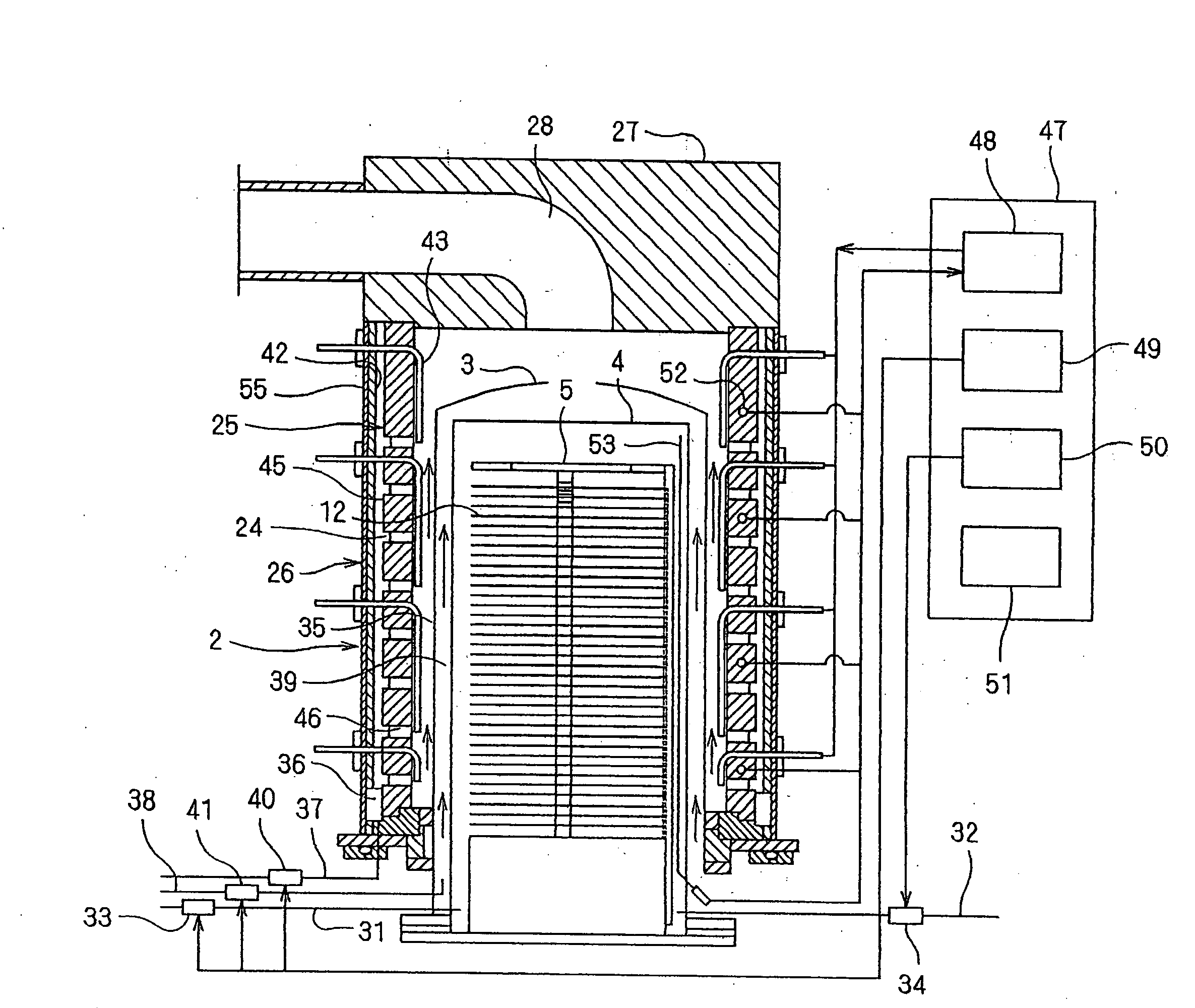
[0037]A thermal equalizer tube 3 and a reactor tube 4 are provided concentrically in a heating module 2 of a tubular shape. The reactor tube 4 has a processing chamber provided therein where a boat 5 is installed to carry a group of horizontally placed wafers 12 in layers. The boat 5 can be loaded in and out from the processing chamber by the action of a boat elevator not shown.

[0038]The reactor tube 4 is communicated with a reactive gas supply conduit 31 and an exhaust conduit 32. A flow controller 33 is provided across the reactive gas supply conduit 31 while a pressure controller 34 is provided across the exhaust conduit 32. This allows each reactive gas to be in...


PUM


Abstract

A substrate treating device comprising a treatment chamber for storing and treating substrates and a heating device having a heating element and a heat insulator and heating the substrates in the treatment chamber by the heating element. The heating element is so formed that only its one end is held by a holding part, and a projection projected to the treatment chamber side at the intermediate part of the heating element and positioned in proximity to or in contact with the heating element is formed on the heat insulator. A pin with an enlarged part is passed through the heating element and the heat insulator at the intermediate part of the heating element and The enlarged part is positioned in proximity to or in contact with the heating element. The plurality of projections may be formed on the heat insulator and the pins may be disposed between these plurality of projections.

Description

TECHNICAL FIELD[0001]The present invention relates to a substrate processing apparatus for producing semiconductor devices on a substrate such as a silicon wafer or a glass substrate, a heating apparatus for use in the substrate processing apparatus, a method of manufacturing semiconductors with those apparatuses, and a heating element supporting structure.DESCRIPTION OF THE RELATED ART[0002]Among the apparatuses for producing semiconductor devices is a substrate processing apparatus designed for conducting deposition of thin layers, annealing, diffusion of impurities, and etching processed over a substrate such as a silicon wafer or a glass substrate. Such a substrate processing apparatus is classified into a multiple type for processing one or more wafers in a sequence and a batch type for processing prescribed numbers of wafers at once. The batch type substrate processing apparatus is also classified into a vertical type employing a vertical furnace and a horizontal type employin...

Claims


Application Information

Patent Timeline
Patent Type & Authority Applications(United States)
IPC IPC(8): H01L21/31A21B1/00
CPCH01L21/67109H01L21/324H01L21/22H01L21/205H05B3/64
Inventor MIYATA, TOSHIMITSUHAYASHIDA, AKIRASHIMADA, MASAKAZUKITAMURA, KIMIOTANAKA, KENJI
Owner KOKUSA ELECTRIC CO LTD
Why Eureka
Try Eureka