Method to Reduce Static Phase Errors and Reference Spurs in Charge Pumps

Inactive Publication Date: 2009-02-12
IBM CORP
View PDF9 Cites 10 Cited by
  • Summary
  • Abstract
  • Description
  • Claims
  • Application Information

AI Technical Summary

Benefits of technology

[0023]Advantages of the design provided herein include, without limitation: cancellation logic located between a phase frequency detector (PFD) and charge pump removes undesired equal value pulses; orthogonal control of charge pump mismatch and charge pump gain; digital cancellation circuitry is virtually independent of process-temperature-voltage (PVT) variations; undesired equal value pulses are removed at the source; simple and efficient design; there is a significant reduction of area and power consumption; and, a 3rd order loop filter is not required to damp reference spurs. Further, the design is suitable for very wideband PLLs because the (analog based) prior-art methods may exhibit operational difficulties in PLL rail-to-rail performance providing sufficiently suppressed charge feed-through.
[0024]As a result of the summarized invention, technically we have achieved a solution which a computer program product stored on machine readable media, including instructions for implementing a phase-locked-loop (PLL) circuit, is provided. The product includes instructions for: providing a differen

Problems solved by technology

However, if the inputs are slightly mismatched, either the up or down pulse will contain slightly more charge than the other and the PLL needs to correct that mismatch.
During the pulse width of the short pulses both charge pump paths—the sourcing and sinking path—are active and may lead to a deteriorated performance (charge feed-through, ripples, increased phase noise and jitter) if some loop components are non-ideal.
Static phase errors—defined as the residual phase error of the input signals of the phase detector when the PLL is in the locked state—may lead to severe phase noise degradation and jitter peaking in PLL circuits.
Second of all, there is charge pump mismatch.
More specifically, current sourcing and sinking in the charge pump is not sufficiently matched (e.g. because of different threshold voltages and electron mobility of the PMOS and NMOS current sources).
In addition, there is

Method used


Image

  • Method to Reduce Static Phase Errors and Reference Spurs in Charge Pumps
  • Method to Reduce Static Phase Errors and Reference Spurs in Charge Pumps
  • Method to Reduce Static Phase Errors and Reference Spurs in Charge Pumps

Examples


Example

[0032]The detailed description explains the preferred embodiments of the invention, together with advantages and features, by way of example with reference to the drawings.

DETAILED DESCRIPTION OF THE INVENTION

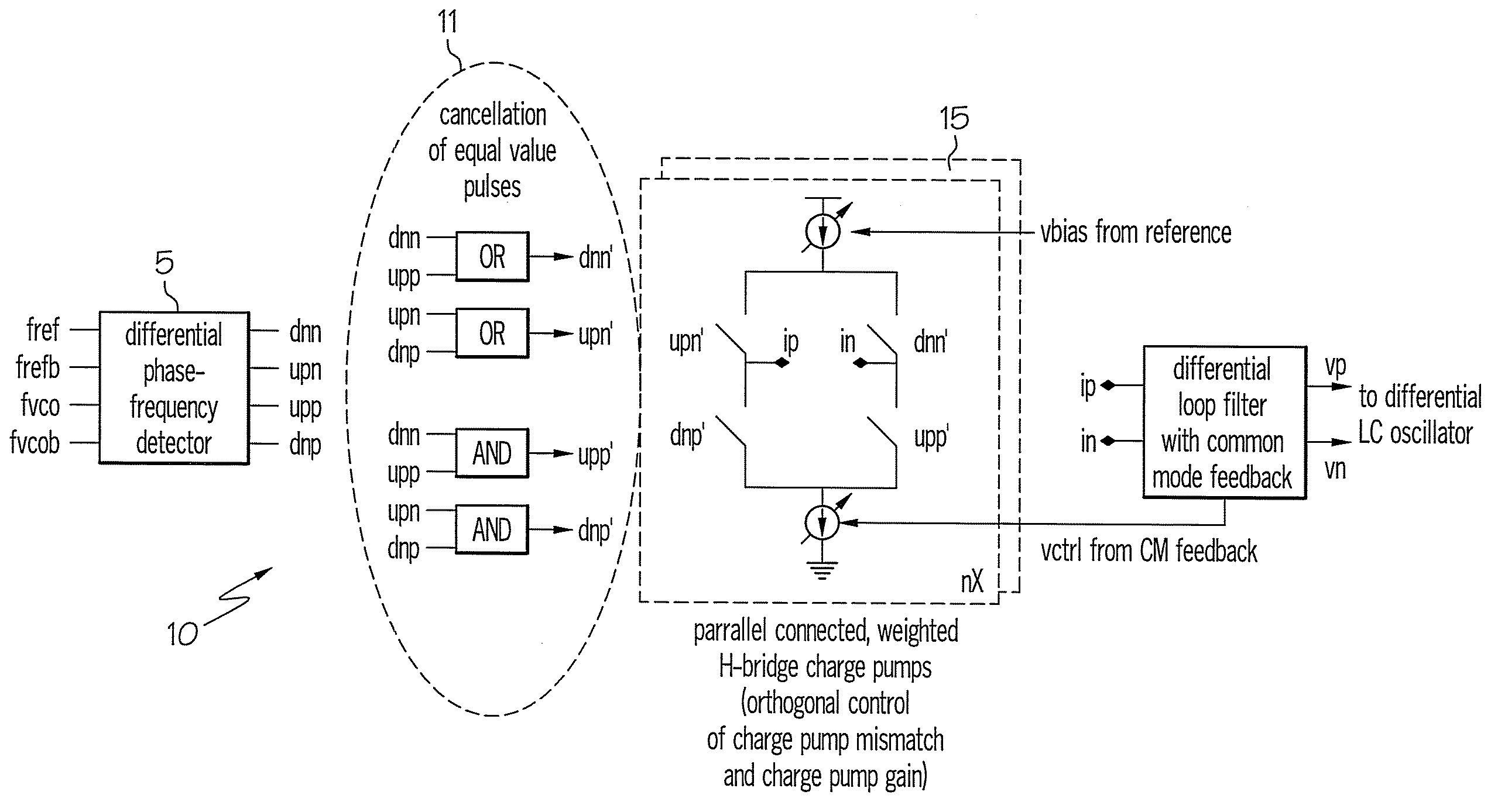
[0033]Disclosed is a design for a phase-locked-loop (PLL) circuit that addresses charge feed-through and charge pump mismatch effects. The design may be applied to delay-locked-loop (DLL) circuits as well. For convenience, an exemplary embodiment is provided in FIG. 3.

[0034]In FIG. 3, aspects of a circuit 10 for cancellation of pulses of substantially equivalent value in order to reduce static phase errors and reference spurs is depicted. The circuit 10 applies logic 11 between a phase-frequency detectors (PFD) 5 and a charge pump 15. The logic 11 conditions control signals of the charge pump 15 in such a way that none of the switches for the charge pump 15 are closed simultaneously. Additionally, a core of the charge pump 15 is extended with an orthogonal adjustment of a gain ...


PUM


Abstract

A phase-locked-loop (PLL) circuit, that includes: a differential phase-frequency detector, a charge pump and at least one logical gate disposed therebetween for providing cancellation of pulses of a substantially equivalent value output by the detector to the charge pump; wherein the at least one logical gate receives the detector output signals and generates control signals for the charge pump such that the pulses of substantially equivalent value are eliminated.

Description

BACKGROUND OF THE INVENTION[0001]1. Field of the Invention[0002]The teachings herein are related to phase-locked-loop (PLL) or delay-locked loop (DLL) circuits, and in particular to techniques for preventing charge feed-through in a charge pump.[0003]2. Description of the Related Art[0004]Analog PLL circuits are generally built of a phase detector, low pass filter and voltage-controlled oscillator (VCO) placed in a negative feedback configuration. There may be a frequency divider in the feedback path or in the reference path, or both, in order to make an output clock of the PLL an integer multiple of the reference path.[0005]Aspects of PLL circuits are discussed in general terms in Wikipedia, an online encyclopedia. Portions of this description of related art are derived from content therein.[0006]The oscillator generates a periodic output signal. Assume that the oscillator is at nearly the same frequency as the reference signal. Then, if the phase from the oscillator falls behind t...

Claims


Application Information

Patent Timeline
IPC IPC(8): H03L7/06G06F1/00
CPCH03L7/089H03L7/0898H03L7/0896
Inventor KOSSEL, MARCEL A.
Owner IBM CORP
Why Eureka
Try Eureka