Solid-state imaging device, imaging apparatus and driving method for the same

a technology of solid-state imaging and imaging apparatus, which is applied in the direction of radio frequency controlled devices, instruments, television systems, etc., can solve the problems of insufficient fixation of the potential of the p-well in the center of the imaging region, inferior results, and generation of false signals, so as to prevent overflowing of charge from the photoelectric conversion elements of the second-group pixels, the effect of reducing the number of frames and reducing the number of operations

Active Publication Date: 2009-02-12
PANASONIC SEMICON SOLUTIONS CO LTD
View PDF4 Cites 8 Cited by
  • Summary
  • Abstract
  • Description
  • Claims
  • Application Information

AI Technical Summary

Benefits of technology

[0037]With this arrangement, the first-group pixels perform electronic shutter operation of limiting the time during which charge is accumulated in the photoelectric conversion elements to a fixed time. As for the second-group pixels skipped during thinning drive, also, the time during which charge is accumulated in the photoelectric conversion elements is made roughly the same as the time of the electronic shutter operation of the first-group pixels. Therefore, overflowing of charge from the photoelectric conversion elements of the second-group pixels can be prevented.
[0038]Thus, according to the present invention, a solid-state imaging device having a high frame rate in which the potential of the p-well is prevented from varying during thinning drive and thus the read and reset operation is shortened can be implemented.

Problems solved by technology

A conventional problem of MOS sensors that the resultant image quality is inferior compared to CCD devices is becoming improved.
Therefore, if the thinning drive is realized by simply not selecting a pixel, a signal overflowing from a photoelectric conversion element of the skipped pixel may flow into an adjacent pixel, possibly causing generation of a false signal.
However, the conventional solid-state imaging device and drive method for such a device described above have the following problem.
In this case, however, the potential of the p-well is not sufficiently fixed in the center of the imaging region.
Thus, since it takes time to perform read and reset operation, a higher frame rate is unobtainable even though pixels are thinned for reading.

Method used


Image

  • Solid-state imaging device, imaging apparatus and driving method for the same
  • Solid-state imaging device, imaging apparatus and driving method for the same
  • Solid-state imaging device, imaging apparatus and driving method for the same

Examples


embodiment 1

Circuit Configuration

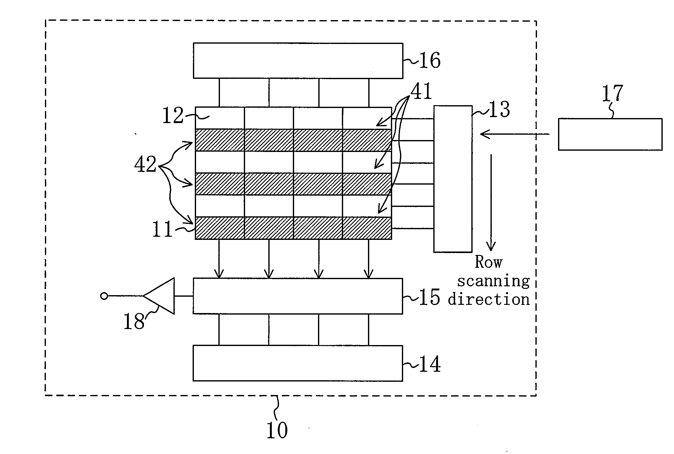
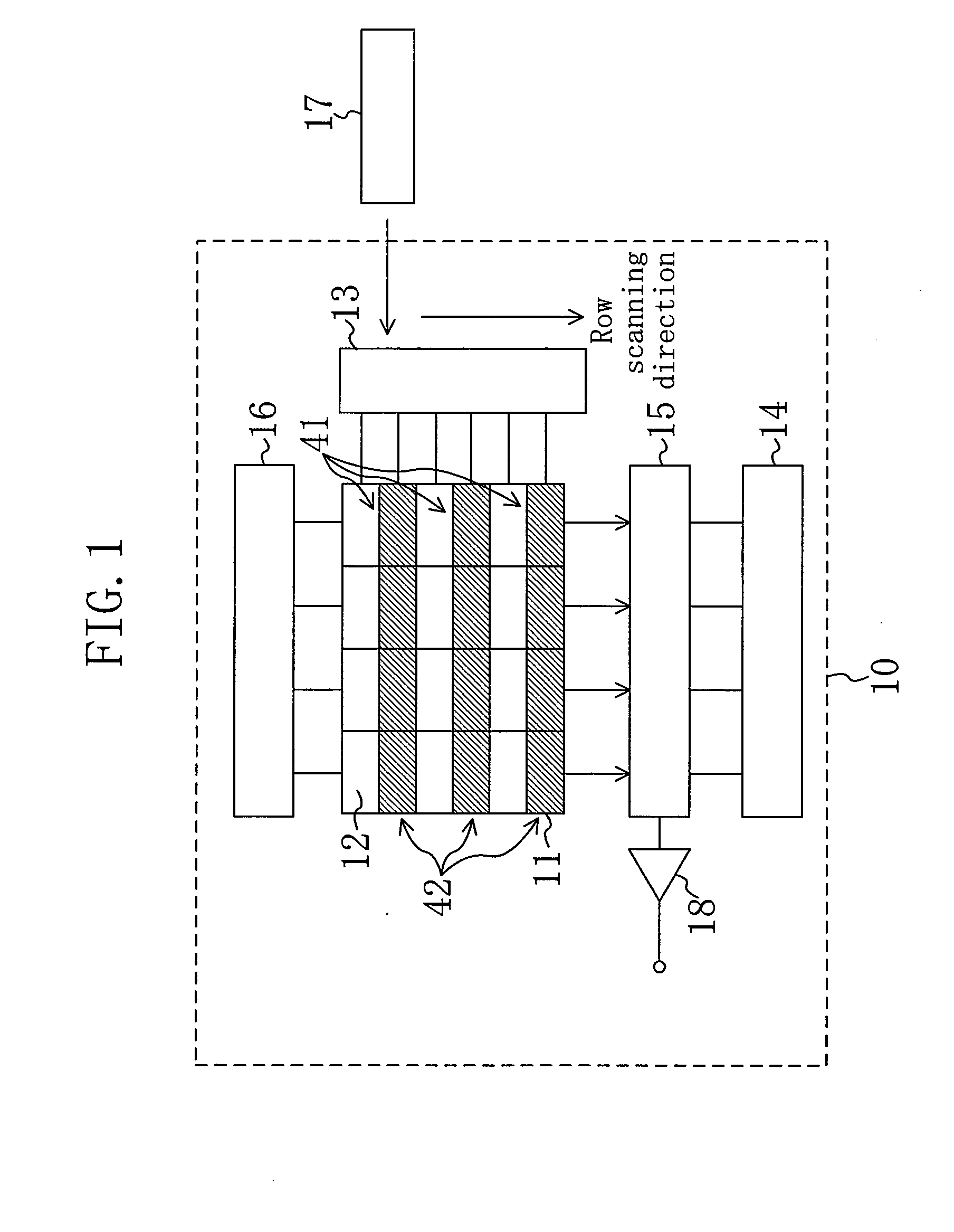
[0104]FIG. 1 shows an outline of a solid-state imaging device of Embodiment 1 of the present invention. As shown in FIG. 1, the solid-state imaging device, denoted by 10, includes an imaging region 11 composed of a plurality of pixels 12 arranged in a matrix. In this embodiment, the pixels 12 include first-group pixels 41 that are read during thinning drive and second-group pixels 42 that are skipped during the thinning drive. Although the first-group pixels 41 and the second-group pixels 42 are arranged every other row in the illustrated example, any other arrangement of these pixels may be adopted.

[0105]Each of the pixels 12 is subjected to read operation and reset operation with a read pulse and a reset pulse supplied from a row scanning section 13. The row scanning section 13, connected to a control section 17, generates control pulses such as a transfer pulse and the reset pulse based on various control signals supplied from the control section 17.

[0106]Sig...

embodiment 2

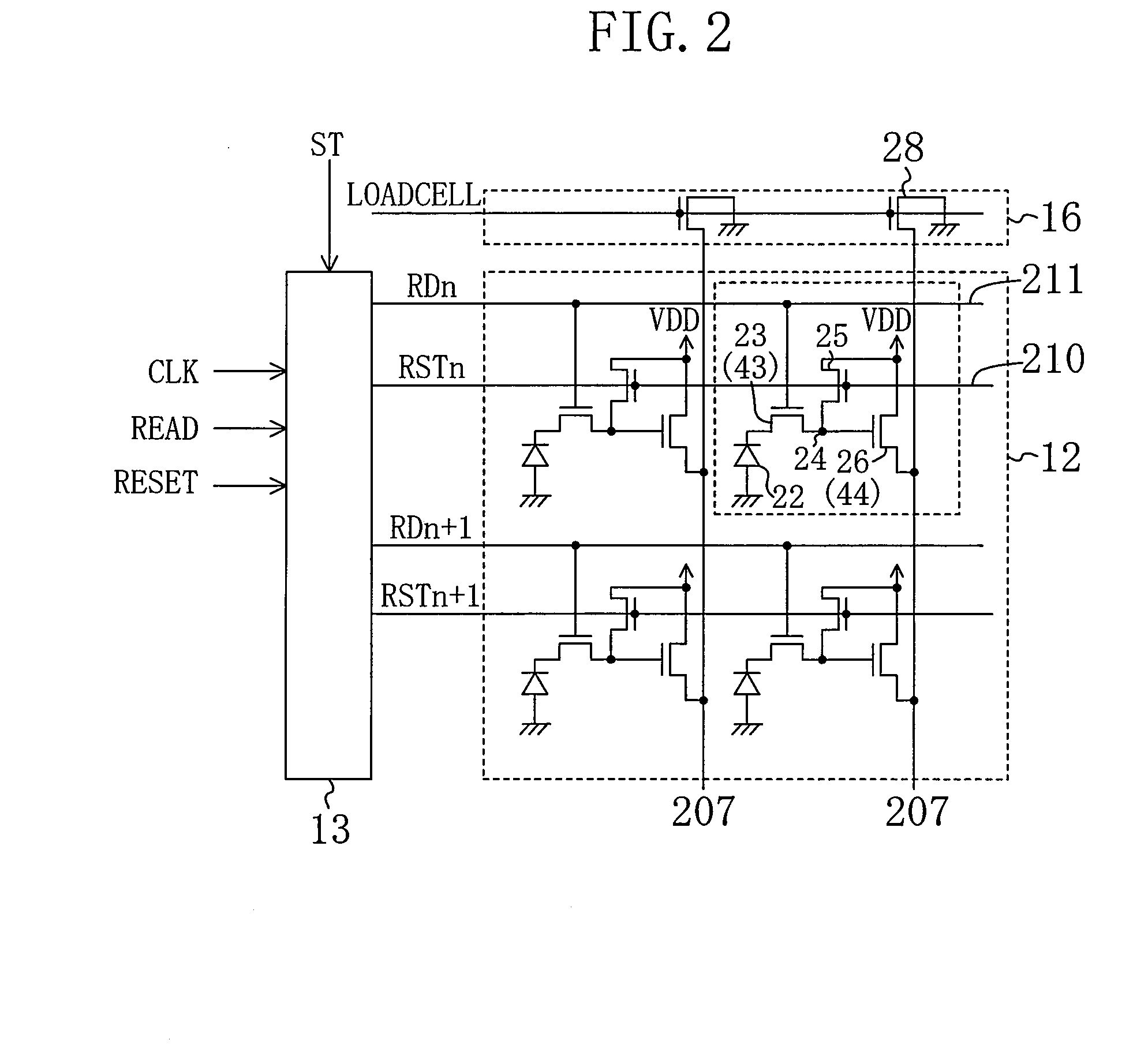
[0151]Embodiment 2 of the present invention will be described with reference to the relevant drawings. FIG. 11 shows a circuit configuration of a main portion of a solid-state imaging device of Embodiment 2. In FIG. 11, the same components as those in FIG. 2 are denoted by the same reference numerals, and the description thereof is omitted here. The entire block configuration of the solid-state imaging device is the same as that of Embodiment 1.

[0152]As shown in FIG. 11, the solid-state imaging device of this embodiment has a read selection transistor 32 and a pull-down transistor 33 for each row. The read selection transistor 32 for the n-th row receives at its gate an output signal Qn from the shift register provided in the row scanning section 13 and receives at its drain a read pulse READ supplied from the control section 17, to thereby supply a transfer pulse RDn for the n-th row to the transfer signal line 211 for the n-th row. The pull-down transistor 33 for the n-th row grou...

embodiment 3

[0163]Embodiment 3 of the present invention will be described with reference to the relevant drawings. FIG. 14 shows a circuit configuration of a main portion of a solid-state imaging device of Embodiment 3. In FIG. 14, the same components as those in FIG. 2 are denoted by the same reference numerals, and the description thereof is omitted here. The entire block configuration of the solid-state imaging device is the same as that of Embodiment 1.

[0164]As shown in FIG. 14, the solid-state imaging device of this embodiment does not include the transfer transistors 23 and the transfer signal lines 211, but instead includes selection transistors 34 and selection signal lines 215.

[0165]The photodiode 22 in each pixel is connected to the source of the reset transistor 25 and the gate of the amplification transistor 26, and the signal output from the amplification transistor 26 is read to the vertical output signal line 207 by switching ON / OFF the selection transistor 34. Therefore, the res...


PUM


Abstract

A solid-state imaging device includes first-group pixels 41, second-group pixels 42 skipped during thinning drive, and a scanning section 13. The scanning section 13 drives each of the first-group pixels 41 to perform read operation of outputting the output signal and initializing the amount of the signal charge accumulated in the photoelectric conversion element to a first level, and also drives each of the second-group pixels 42 to perform discharge operation of initializing the amount of the signal charge accumulated in the photoelectric conversion element to a second level that is higher than the first level and lower than a saturation signal level of the photoelectric conversion element 12.

Description

TECHNICAL FIELD[0001]The present invention relates to a solid-state imaging device, an imaging apparatus and a driving method for such a device, and more particularly, to a solid-state imaging device and an imaging apparatus for high-speed moving-picture imaging, and a driving method for such a device.BACKGROUND ART[0002]In recent years, MOS sensors operable at low voltage have attracted attention in their application to portable equipment and the like. A conventional problem of MOS sensors that the resultant image quality is inferior compared to CCD devices is becoming improved.[0003]To achieve both high-definition still-picture imaging and high-speed moving-picture imaging with one MOS sensor, a solid-state imaging device that performs thinning drive in which pixels in the MOS sensor are thinned in reading has been developed.[0004]In a solid-state imaging device made of a MOS sensor, which can read only signals from pixels to which a selection pulse has been supplied, the thinning...

Claims


Application Information

Patent Timeline
Patent Type & Authority Applications(United States)
IPC IPC(8): H04N5/335H04N5/225H04N5/341H04N5/345H04N5/359H04N5/361H04N5/374H04N5/3745
CPCH04N3/1562H04N25/445H04N25/745H04N25/62H04N25/76
Inventor MASUYAMA, MASAYUKIHARA, KUNIHIKOMURAKAMI, MASASHINEZAKI, SHINSUKE
Owner PANASONIC SEMICON SOLUTIONS CO LTD
Why Eureka
Try Eureka