Method and structure using selected implant angles using a linear accelerator process for manufacture of free standing films of materials

a technology of free standing films and accelerator processes, which is applied in the direction of semiconductor/solid-state device manufacturing, basic electric elements, electric apparatus, etc., can solve the problems of not possessing the optimum properties of highly effective solar cells, materials are often difficult to manufacture, and many limitations of solar cells, so as to increase the stress level of the cleave region

Inactive Publication Date: 2009-02-12
SILICON GENERAL CORPORATION
View PDF10 Cites 34 Cited by
  • Summary
  • Abstract
  • Description
  • Claims
  • Application Information

AI Technical Summary

Benefits of technology

[0016]In still further embodiments, the present invention provides still another method for fabricating free standing thickness of materials using one or more semiconductor substrates. In a specific embodiment, the present method includes providing a semiconductor substrate having a surface region and a thickness. The method includes subjecting the surface region of the semiconductor substrate to a first plurality of high energy particles comprising D+species generated using a linear accelerator to form a plurality of gettering sites within a cleave region, which is provided beneath the surface region to defined a thickness of material to be detached. The method includes subjecting the semiconductor substrate to a treatment process according to a specific embodiment. The method includes subjecting the surface region of the semiconductor substrate to a second plurality of high energy particles comprising H2+ species using the linear accelerator, which is preferably the same linear accelerator as the one providing the D+ species. In a specific embodiment, the second plurality of high energy particles are provided to increase a stress level of the cleave region from a first stress level to a second stress level. The method includes initiating the cleaving action at a selected region of the cleave region to detach a portion of the thickness of detachable material using a cleaving process. The method includes freeing the thickness of detachable material.

Problems solved by technology

Unfortunately, such petroleum sources have become depleted and have lead to other problems.
Although effective, these solar cells still have many limitations.
These materials are often difficult to manufacture.
Although these plates may be formed effectively, they do not possess optimum properties for highly effective solar cells.
Such single crystal silicon is, however, expensive and is also difficult to use for solar applications in an efficient and cost effective manner.
Additionally, both polysilicon and single-crystal silicon materials suffer from material losses during conventional manufacturing called “kerf loss”, where the sawing process eliminates as much as 40% and even up to 60% of the starting material from a cast or grown boule and singulate the material into a wafer form factor.
This is a highly inefficient method of preparing thin polysilicon or single-crystal silicon plates for solar cell use.
Generally, thin-film solar cells are less expensive by using less silicon material but their amorphous or polycrystalline structure are less efficient than the more expensive bulk silicon cells made from single-crystal silicon substrates.

Method used


Image

  • Method and structure using selected implant angles using a linear accelerator process for manufacture of free standing films of materials
  • Method and structure using selected implant angles using a linear accelerator process for manufacture of free standing films of materials
  • Method and structure using selected implant angles using a linear accelerator process for manufacture of free standing films of materials

Examples


examples

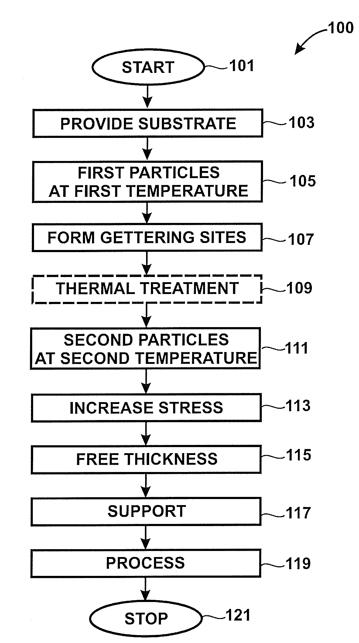
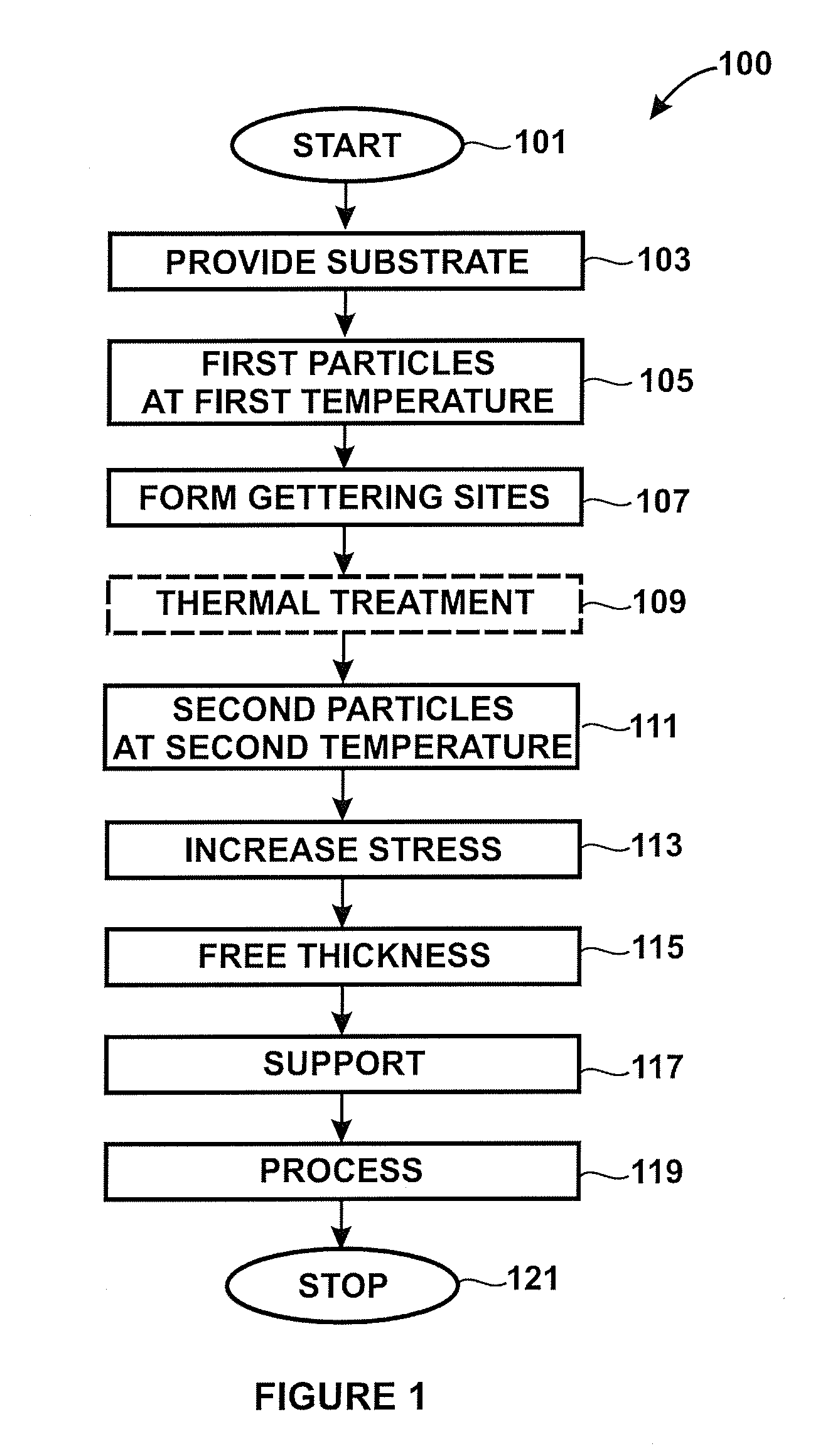
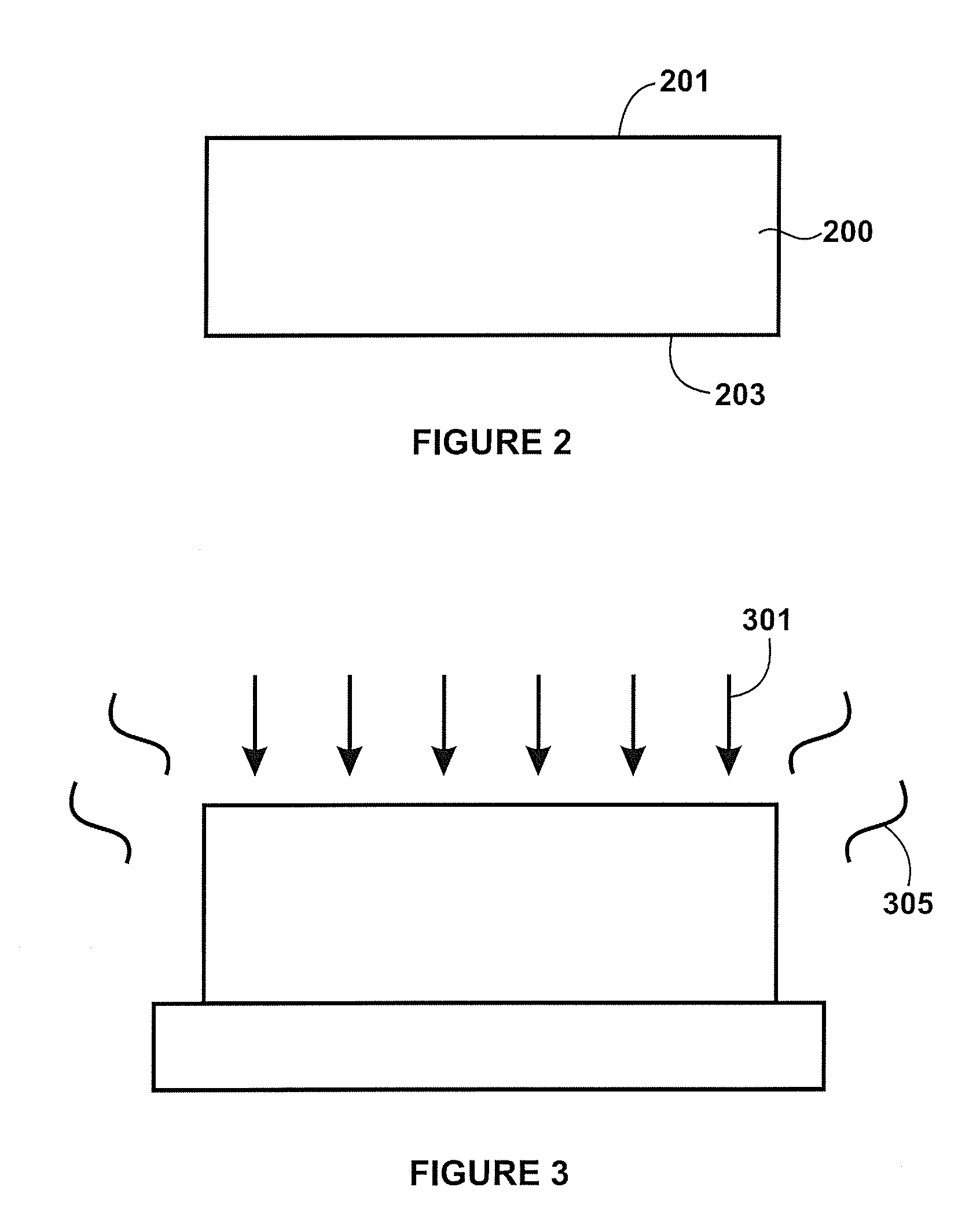
[0151]To prove the principles and operation of the present invention, we perform certain experiments. These experiments are merely examples, which should not unduly limit the scope of the claims herein. One of ordinary skill in the art would recognize many other variations, modifications, alternatives. Further details of these experiments can be found throughout the present specification and more particularly below.

[0152]As an example, silicon wafer samples were prepared having various orientations and impurities. In a specific embodiment, square shaped samples, which were orientation and p-type doped, were prepared. In an alternative embodiment, round shaped samples, which were orientation and n-type doped, were prepared. Depending upon the embodiment and experiments, we can use other variations, modifications, and alternatives. Additionally, the square and round shape lead to certain characteristics but should be used herein for labeling purposes and shall not unduly limit the s...


PUM

PropertyMeasurementUnit
angleaaaaaaaaaa
angleaaaaaaaaaa
angleaaaaaaaaaa

Abstract

A method for fabricating free standing thickness of materials using one or more semiconductor substrates, e.g., single crystal silicon, polysilicon, silicon germanium, germanium, group III/IV materials, and others. In a specific embodiment, the present method includes providing a semiconductor substrate having a surface region and a thickness. The method includes subjecting the surface region of the semiconductor substrate to a first plurality of high energy particles provided at a first implant angle generated using a linear accelerator to form a region of a plurality of gettering sites within a cleave region, the cleave region being provided beneath the surface region to defined a thickness of material to be detached, the semiconductor substrate being maintained at a first temperature. In a specific embodiment, the method includes subjecting the surface region of the semiconductor substrate to a second plurality of high energy particles at a second implant angle generated using the linear accelerator, the second plurality of high energy particles being provided to increase a stress level of the cleave region from a first stress level to a second stress level. In a preferred embodiment, the semiconductor substrate is maintained at a second temperature, which is higher than the first temperature. The method frees the thickness of detachable material using a cleaving process, e.g., controlled cleaving process.

Description

CROSS-REFERENCE TO RELATED APPLICATION[0001]The instant nonprovisional patent application claims priority to U.S. Provisional Patent Application No. 60 / 887,086, filed Jan. 29, 2007 and incorporated by reference herein for all purposes.BACKGROUND OF THE INVENTION[0002]The present invention relates generally to technique including a method and a structure for forming substrates using a layer transfer technique. More particularly, the present method and system provides a method and system using a linear accelerator process for the manufacture of thick free standing semiconductor films for a variety of applications including photovoltaic cells. But it will be recognized that the invention has a wider range of applicability; it can also be applied to other types of applications such as for three-dimensional packaging of integrated semiconductor devices, photonic or optoelectronic devices, piezoelectronic devices, flat panel displays, microelectromechanical systems (“MEMS”), nano-technolo...

Claims


Application Information

Patent Timeline
Patent Type & Authority Applications(United States)
IPC IPC(8): H01L21/263
CPCH01L21/26586H01L21/26506H01L21/2658H01L21/26593
Inventor HENLEY, FRANCOIS J.
Owner SILICON GENERAL CORPORATION
Why Eureka
Try Eureka