Method of fabricating a semiconductor device

a semiconductor device and manufacturing method technology, applied in the direction of solid-state devices, coatings, chemical vapor deposition coatings, etc., can solve the problems of signal interference, hinder the integration and high speed of a semiconductor device, interconnection delay, etc., to improve the overall reliability of the semiconductor device, improve the effect of chemical vapor deposition and improve the reliability

Active Publication Date: 2009-02-12
SAMSUNG ELECTRONICS CO LTD
View PDF4 Cites 16 Cited by
  • Summary
  • Abstract
  • Description
  • Claims
  • Application Information

AI Technical Summary

Benefits of technology

[0014]According to the method of fabricating a semiconductor device according to exemplary embodiments of the present invention, by depositing an insulating layer for isolating wirings using a thermal chemical vapor deposition method that is performed at a relatively high temperature, impurities that can be induced from a reaction gas and dispersed in a subsequent process, can be included in lesser amounts in the insulating layer in comparison to the conventional art. Thus, the overall reliability of the semico

Problems solved by technology

Capacitive coupling due to a parasitic capacitance generated by the metal wirings and a dielectric layer for isolating the metal wirings may cause an interconnection delay that hinders the integration and high speed of a semiconductor device.
In addition to the interconnection delay, signal interference due to the capacitive coupling ma

Method used


Image

  • Method of fabricating a semiconductor device
  • Method of fabricating a semiconductor device
  • Method of fabricating a semiconductor device

Examples


Embodiment Construction

[0019]Exemplary embodiments of the present invention are described below in detail with reference to the attached drawings.

[0020]The exemplary embodiments of the present invention are provided to a person skilled in the art in the technical field to which the present invention pertains for better explanation of the present invention. The following exemplary embodiments may be modified to various types and the scope of the present invention is not limited to the following embodiments.

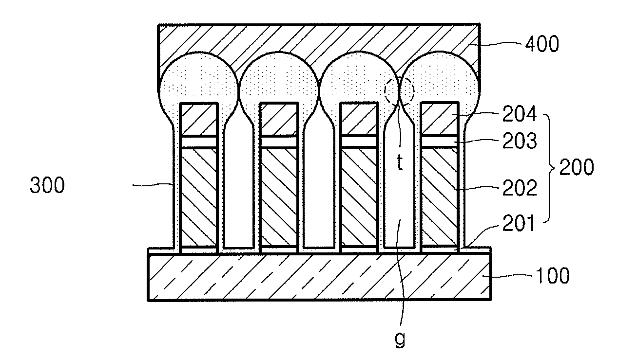
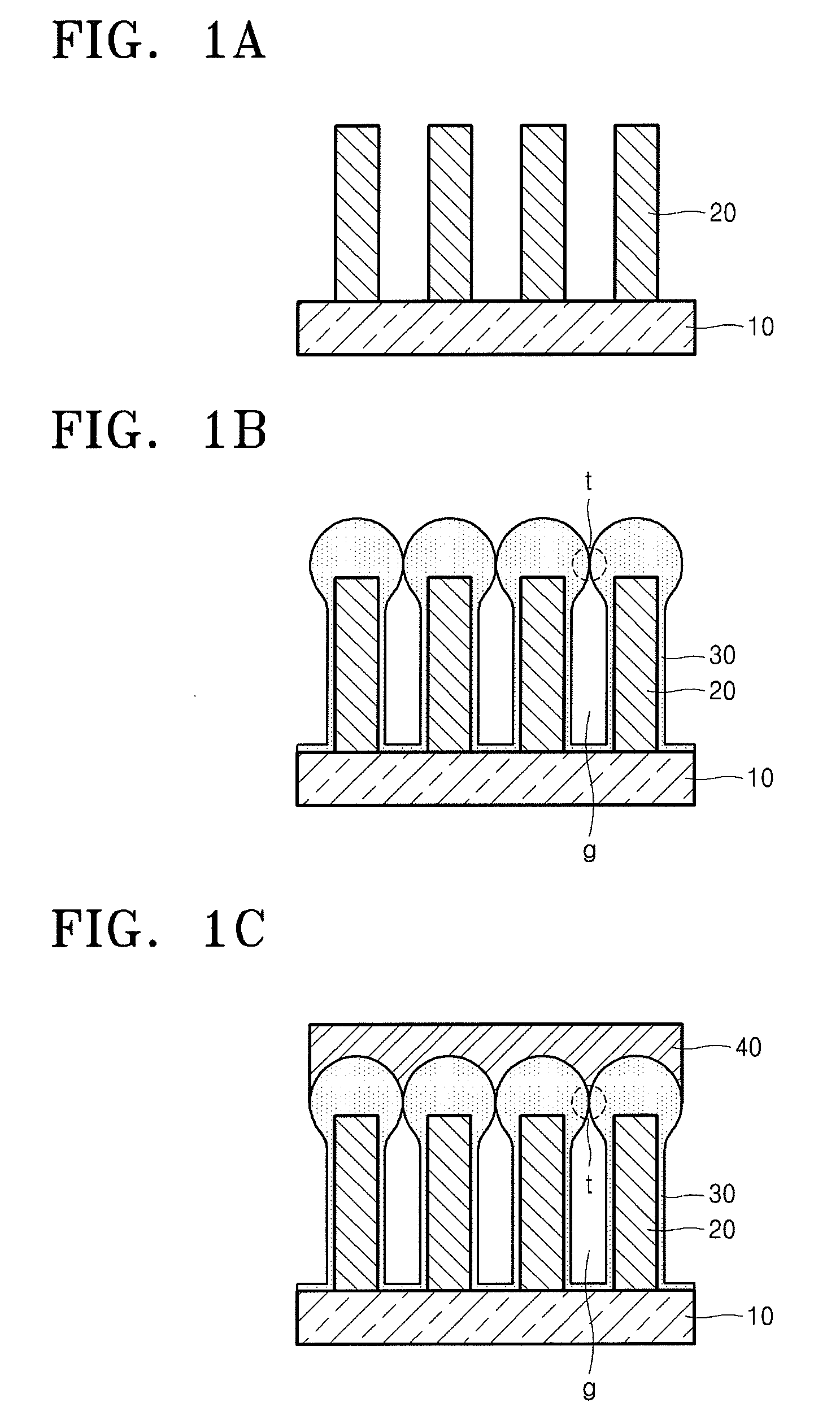
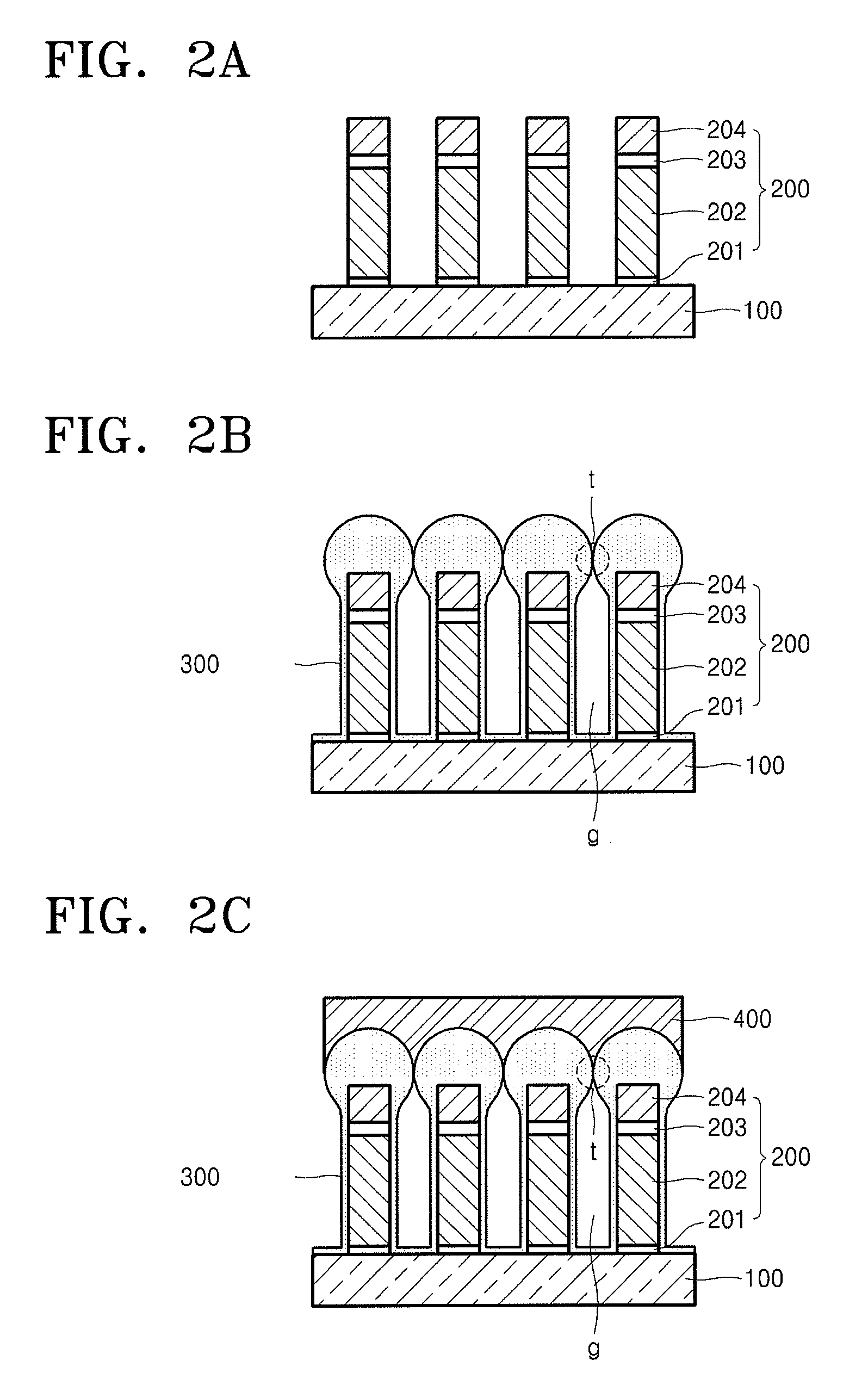
[0021]In the following description, when a layer is described to exist on another layer, this means that the layer may exist directly on the other layer or a third layer may be interposed therebetween. Also, in the drawings, the thickness or size of each layer is exaggerated for the convenience and clarity of explanation and like reference numerals denote like elements. As in the present specification, the term “and / or” includes any one of listed items or one or more combination thereof.

[0022]The terms u...


PUM

PropertyMeasurementUnit
Temperatureaaaaaaaaaa
Pressureaaaaaaaaaa

Abstract

A method of forming a dielectric layer having an air gap to isolate adjacent wirings or a gate stack of the semiconductor device is provided. A method of fabricating a semiconductor device includes providing a semiconductor substrate on which a plurality of wirings are formed adjacent to one another and forming a dielectric layer filling an upper portion of a space between the adjacent wirings to form air gaps by a thermal chemical vapor deposition method.

Description

CROSS-REFERENCE TO RELATED PATENT APPLICATIONS[0001]This application claims the benefit of Korean Patent Application No. 10-2007-0078706, filed on Aug. 6, 2007, the disclosure of which is hereby incorporated by reference herein in its entirety.BACKGROUND OF THE INVENTION[0002]1. Technical Field[0003]The present disclosure relates to a method of fabricating a semiconductor device, and more particularly, to a method of forming a semiconductor device with a dielectric layer having an air gap to isolate wirings or a gate stack of the semiconductor device.[0004]2. Description of the Related Art[0005]As semiconductor devices such as logic elements, DRAMs, or flash memories are typically highly integrated, the distance between metal wirings in the semiconductor devices may gradually decrease. Capacitive coupling due to a parasitic capacitance generated by the metal wirings and a dielectric layer for isolating the metal wirings may cause an interconnection delay that hinders the integration...

Claims


Application Information

Patent Timeline
IPC IPC(8): H01L21/4763
CPCC23C16/402H01L29/4991H01L21/02211H01L21/02271H01L21/02362H01L21/28273H01L21/28282H01L21/31629H01L21/31633H01L21/3185H01L21/764H01L21/7682H01L27/11521H01L27/11568H01L29/4983H01L21/02126H01L29/40114H01L29/40117H10B43/30H10B41/30H01L21/31
Inventor KIM, JIN GYUNKOO, BON-YOUNGHWANG, KI-HYUN
Owner SAMSUNG ELECTRONICS CO LTD
Why Eureka
Try Eureka