

Polishing apparatus, substrate manufacturing method, and electronic apparatus manufacturing method
- Summary
- Abstract
- Description
- Claims
- Application Information
AI Technical Summary
Benefits of technology
Problems solved by technology
Method used
Image

Examples
Embodiment Construction
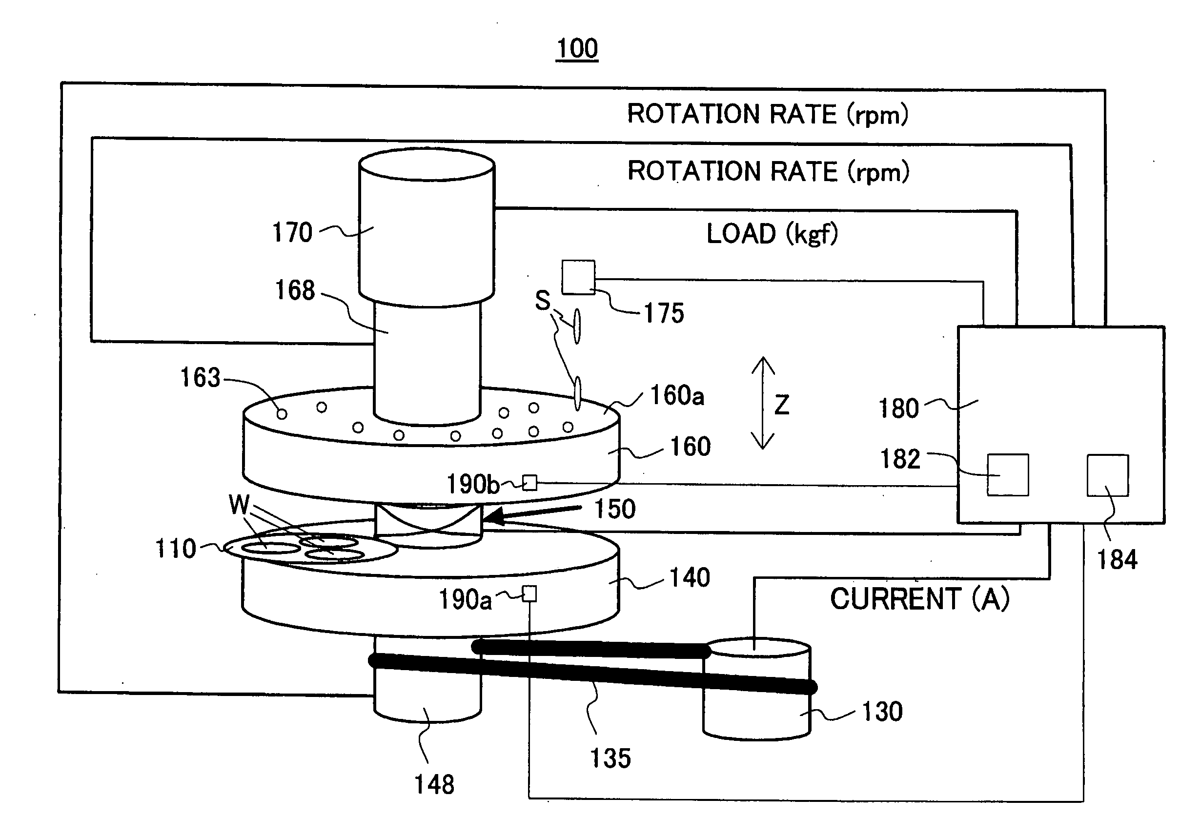
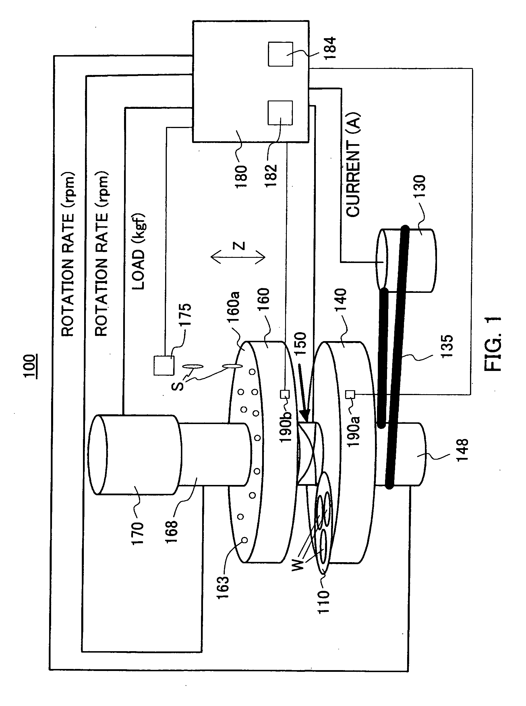
[0054]Referring now to the accompanying drawings, a description will be given of a polishing apparatus 100 according to one embodiment of the present invention. FIG. 1 is a schematic perspective view of a polishing apparatus 100. The polishing apparatus 100 is configured to chemically and mechanically polish both surfaces of a work W simultaneously, but the polishing apparatus of the present invention is applicable to any polishing apparatuses in addition to the CMP apparatus, such as a polishing apparatus for finishing.
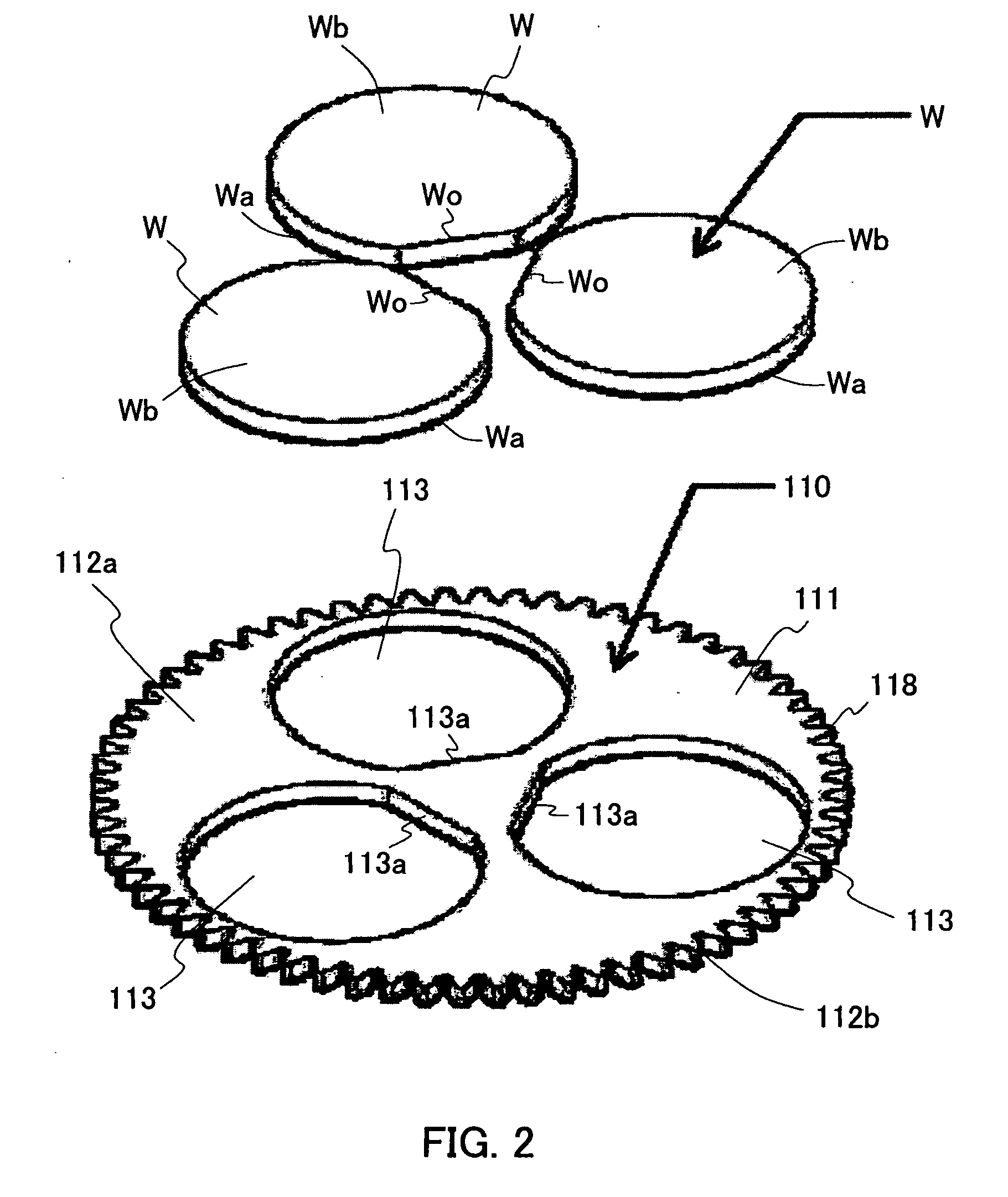
[0055]The work W of this embodiment is a substrate that is a target to be polished. The substrate includes a glass substrate, a silicon substrate, a ceramic substrate (including a laminate substrate), and any other substrates made of a single crystal material. A typical shape of those substrates is a disk shape (a disk shape with an orientation flat if the substrate is a wafer) or a rectangular plate shape. Usually, the substrate has a diameter or length of about doz...
PUM
 Abstract
Description
Claims
Application Information