Nitride semiconductor device

a semiconductor and nitride technology, applied in the direction of semiconductor lasers, solid-state devices, lasers, etc., can solve the problems of lowering the recombination rate of desired light emission inside the active layer, and achieve the effect of increasing the capture rate of carriers in the active layer and enhancing the recombination efficiency

Active Publication Date: 2009-02-19
SAMSUNG ELECTRONICS CO LTD
View PDF4 Cites 54 Cited by
  • Summary
  • Abstract
  • Description
  • Claims
  • Application Information

AI Technical Summary

Benefits of technology

[0010]An aspect of the present invention provides a nitride semiconductor device having an active layer of a superlattice structure, thereby enhancing recombination efficiency and increasing a capture rate of carriers in the active layer.

Problems solved by technology

However, the electrons and holes, if non-uniform with respect to each other in mobility, cause some carriers not to be recombined in the active layer, thereby lowering a recombination rate for desired light emission inside the active layer.

Method used


Image

  • Nitride semiconductor device
  • Nitride semiconductor device
  • Nitride semiconductor device

Examples


Embodiment Construction

[0023]Exemplary embodiments of the present invention will now be described in detail with reference to the accompanying drawings.

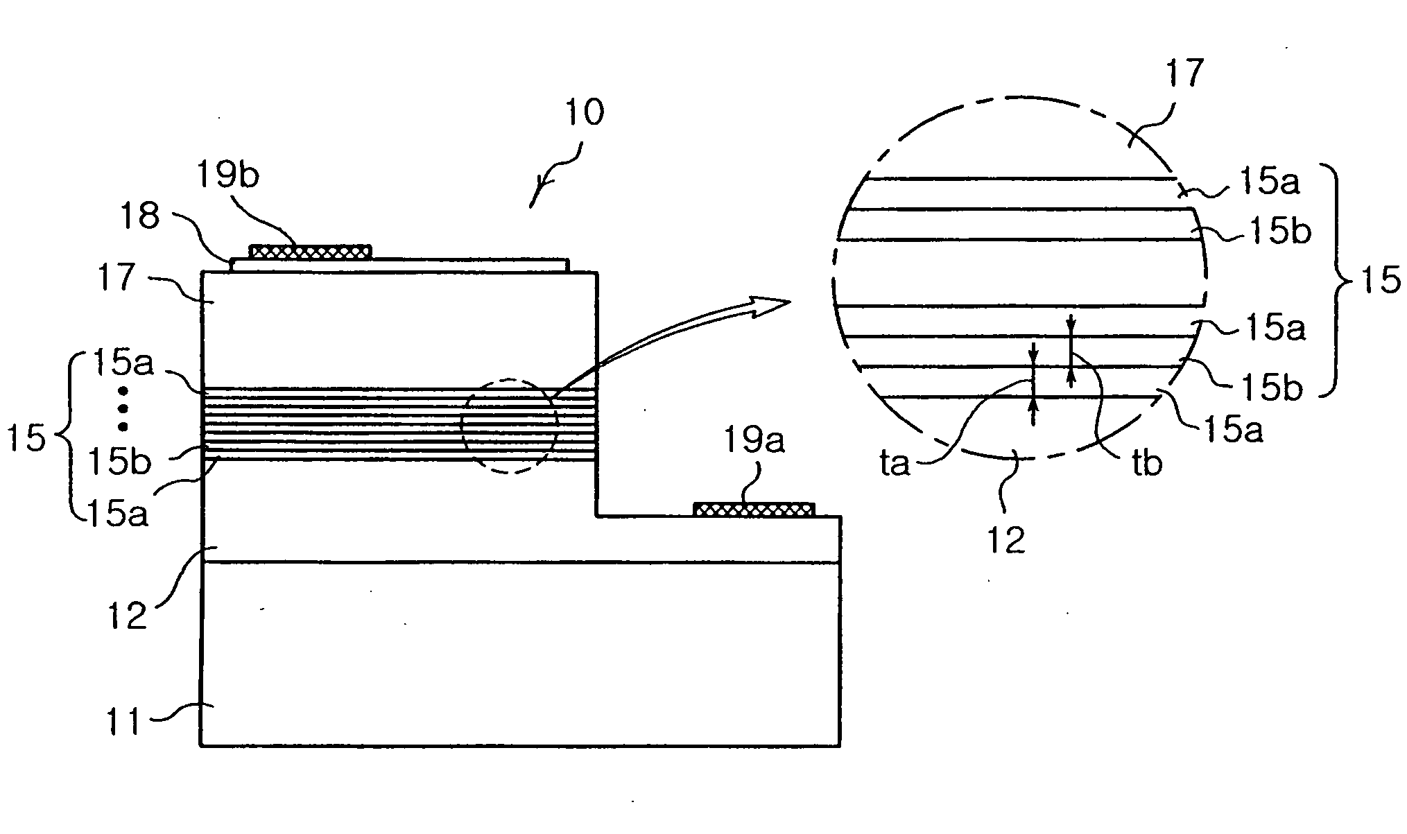
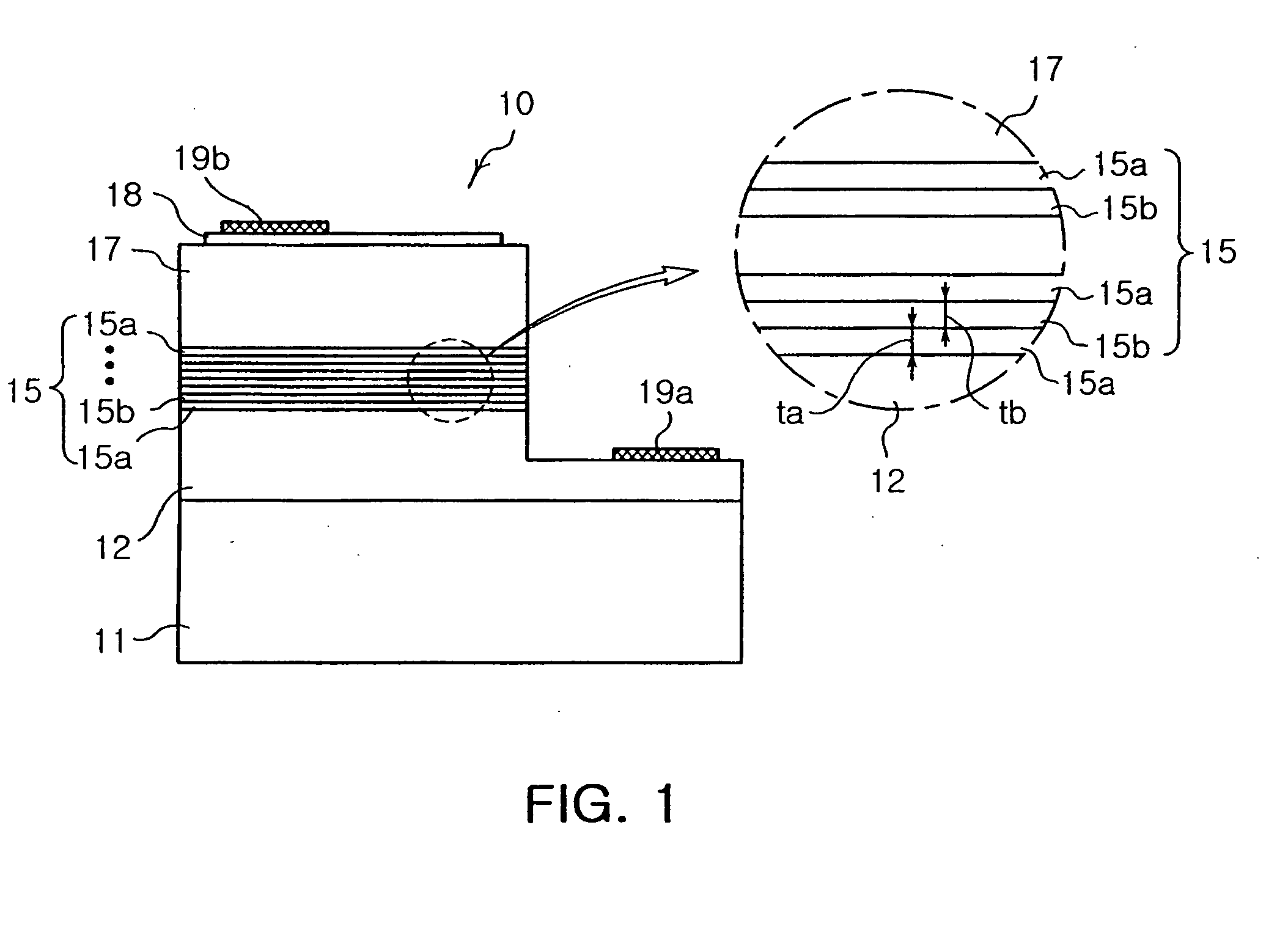
[0024]FIG. 1 is a side cross-sectional view illustrating a nitride semiconductor device according to an exemplary embodiment of the invention.

[0025]As shown in FIG. 1, the nitride semiconductor device includes a substrate 11, an n-type nitride semiconductor layer 12, an active layer 15, and a p-type nitride semiconductor layer 17. The n-type nitride semiconductor layer 12 is mesa-etched to expose a top surface thereof, and an n-electrode 19a is formed on the exposed top surface of the n-type nitride semiconductor layer 12. A transparent electrode layer 18 is formed on the p-type nitride semiconductor layer 17 and a p-electrode 19b is formed on the transparent electrode layer 18.

[0026]The present embodiment illustrates the semiconductor light emitting device of a planar structure where the electrodes 19a and 19b are disposed to face the same direction. Howe...


PUM


Abstract

There is provided a nitride semiconductor device including an active layer of a superlattice structure. The nitride semiconductor device including: a p-type nitride semiconductor layer; an n-type nitride semiconductor layer; and an active layer disposed between the p-type and n-type nitride layers, the active layer comprising a plurality of quantum barrier layers and quantum well layers deposited alternately on each other, wherein the active layer has a superlattice structure where the quantum barrier layer has a thickness for enabling a carrier injected from the p-type and n-type nitride semiconductor layers to be tunneled therethrough, and at least one of the quantum barrier layers has an energy band gap greater than another quantum barrier layer adjacent to the n-type nitride semiconductor layer.

Description

CROSS-REFERENCE TO RELATED APPLICATIONS[0001]This application claims the priority of Korean Patent Application No. 2006-0134120 filed on Dec. 26, 2006, in the Korean Intellectual Property Office, the disclosure of which is incorporated herein by reference.BACKGROUND OF THE INVENTION[0002]1. Field of the Invention[0003]The present invention relates to a nitride semiconductor device, and more particularly, to a nitride semiconductor device having an active layer of a superlattice structure.[0004]2. Description of the Related Art[0005]In general, a nitride semiconductor is widely used in a green or blue light emitting diode (LED) or a laser diode (LD) serving as a light source for full-color displays, image scanners, various signal systems and optical communication devices. This nitride semiconductor device generates and emits light in an active layer by recombination of electrons and holes.[0006]The active layer features a single quantum well (SQW) structure having a single quantum we...

Claims


Application Information

Patent Timeline
Patent Type & Authority Applications(United States)
IPC IPC(8): H01L33/00H01L33/06H01L33/32H01L33/42
CPCB82Y20/00H01L33/06H01S5/34333H01S5/3407H01S5/3416H01L33/32
Inventor PARK, SEONG EUNKIM, MIN HOHAN, JAE WOONG
Owner SAMSUNG ELECTRONICS CO LTD
Why Eureka
Try Eureka