

Oblong peripheral solder ball pads on a printed circuit board for mounting a ball grid array package
a technology of printed circuit board and peripheral solder ball, which is applied in the direction of printed circuit, sustainable manufacturing/processing, final product manufacturing, etc., can solve the problems of increasing the difficulty of forming the routing in the pcbs for the land pattern, shrinking the size of the bga package, and increasing the demand for smaller and smaller electronic devices, so as to reduce the cost of circuit board fabrication and assembly.
- Summary
- Abstract
- Description
- Claims
- Application Information
AI Technical Summary
Benefits of technology
Problems solved by technology
Method used
Image

Examples
example embodiments
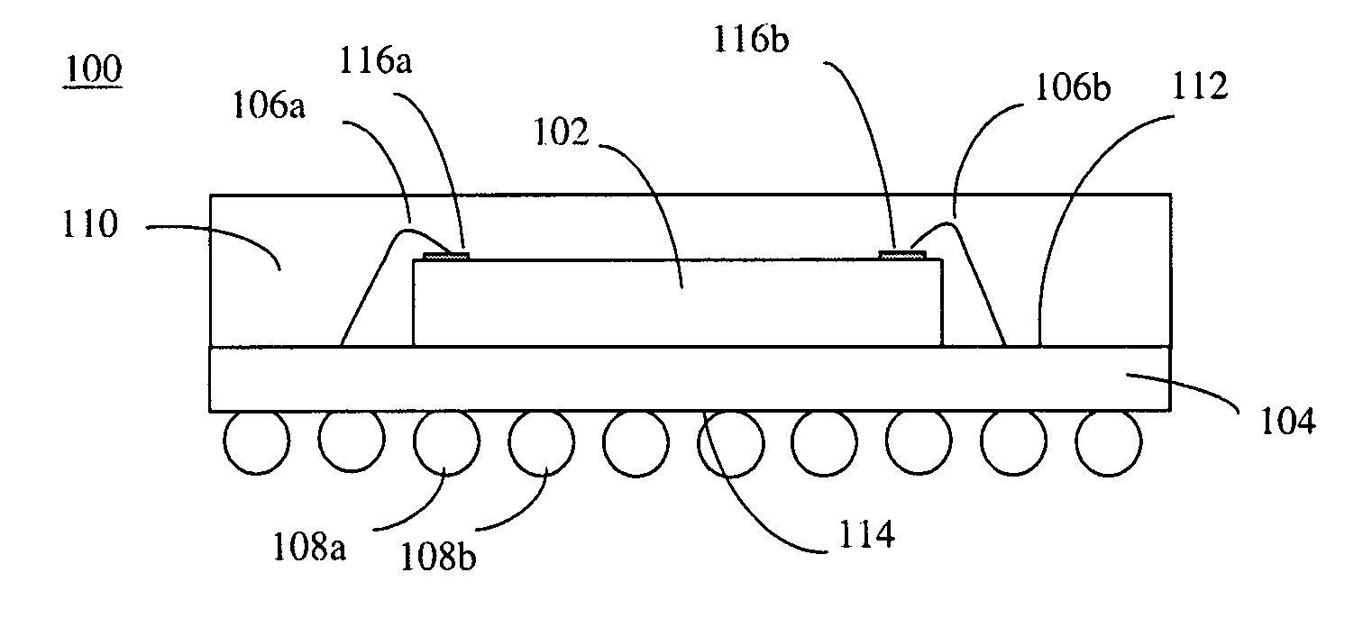
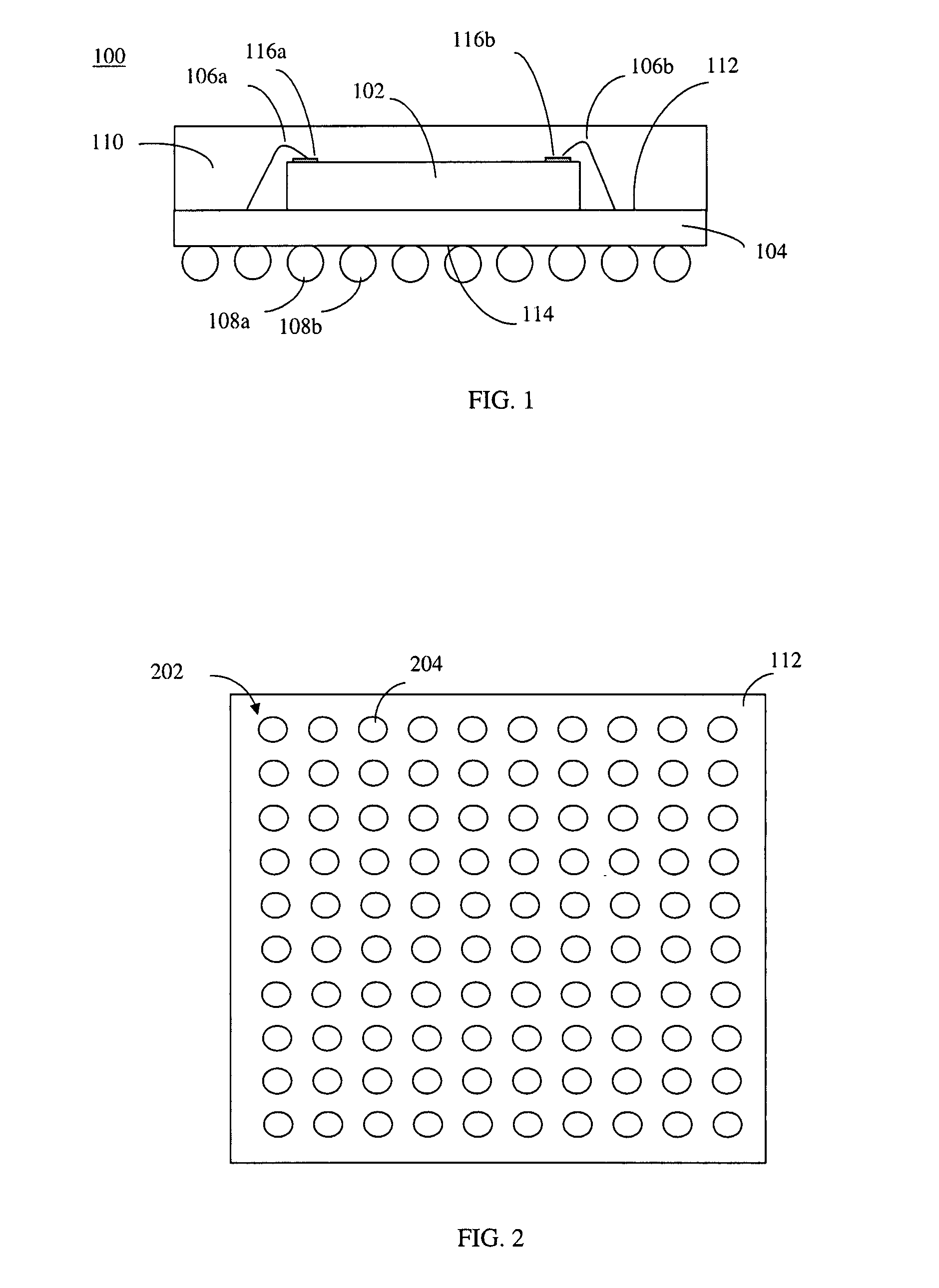
[0053]In embodiments of the present invention, oblong shaped land pads are positioned in a land pattern to enable land pads internal to the land pattern to be routed external to the land pattern using fewer routing layers. The oblong shaped land pads are narrower in width, and thus create additional circuit board space for traces and associated trace clearance requirements. The oblong shaped land pads enable attachment of standard solder balls of a BGA package when the BGA package is mounted to the land pattern. Each oblong shaped land pad provides an electrical connection for a signal from the BGA packages to the circuit board. By enabling attachment of solder balls of a BGA package, the oblong shaped land pads provide mechanical support for attachment of the BGA package to the circuit board.
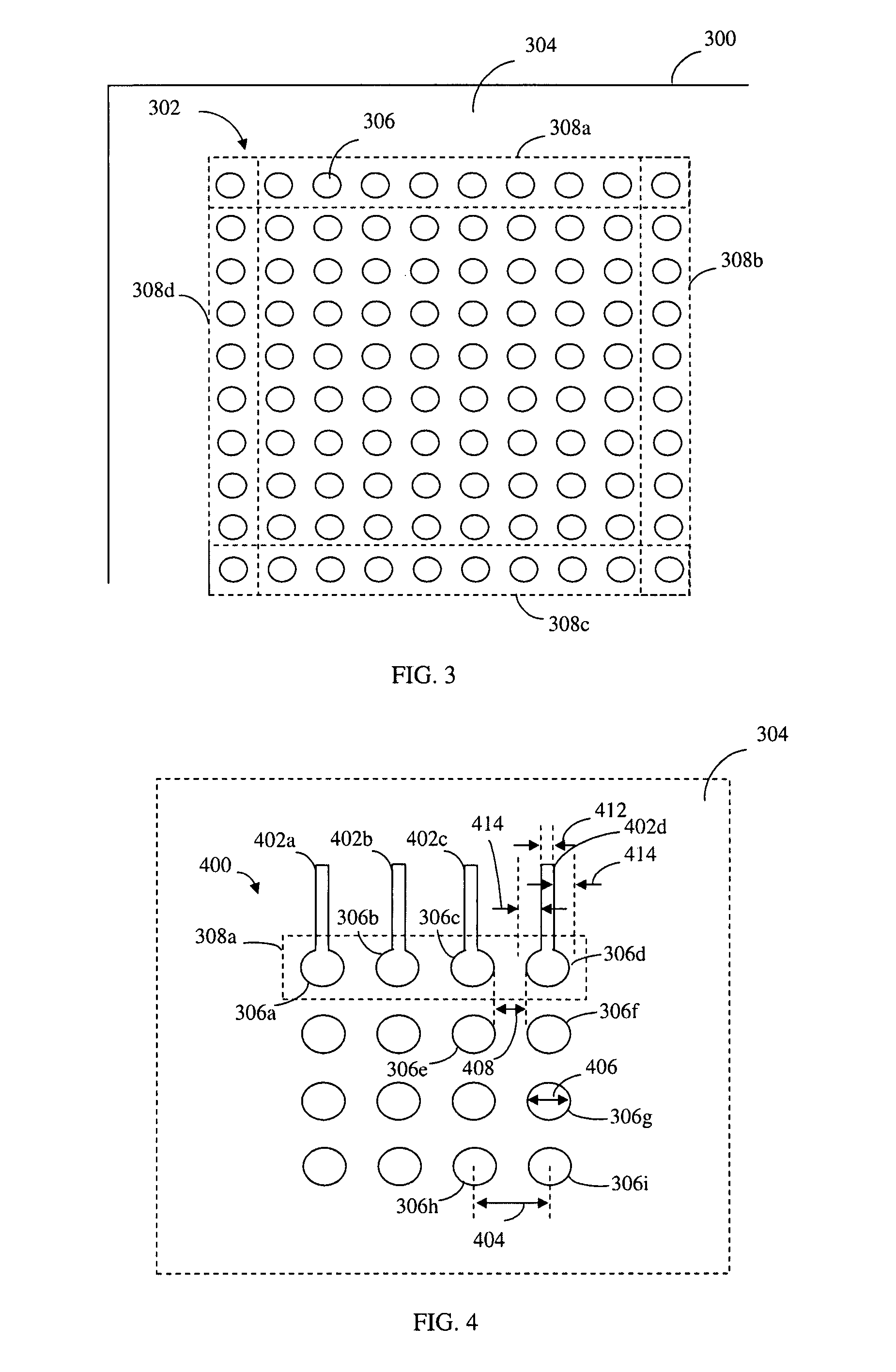
[0054]FIG. 5 shows a portion 500 of a land pattern, according to an example embodiment of the present invention. Portion 500 includes a four by four land pattern array portion. Portion 500 is l...
PUM
 Abstract
Description
Claims
Application Information