[0005]The present invention was made in consideration of the above problems. An object of the present invention is to provide a semiconductor test program debug device capable of reducing the unnecessary facilities when using semiconductor test devices or semiconductor test programs that have different specifications.
[0006]In order to solve the above described problems, a semiconductor test program debug device according to the present invention performs
verification of a semiconductor test program by emulating operations of a semiconductor test device that conducts a test with respect to a
device under test based on the semiconductor test program, and comprises a
virtual device that simulates the operations of the
device under test; a
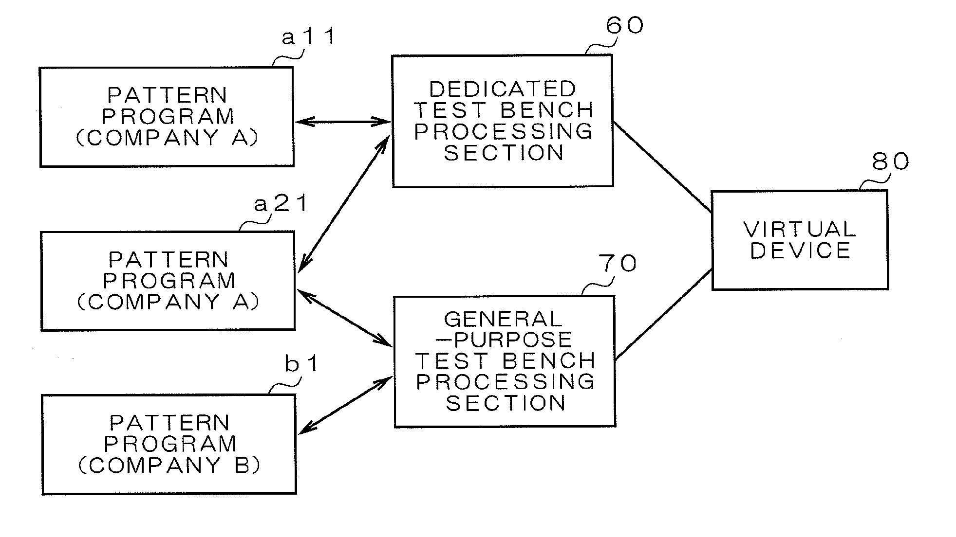
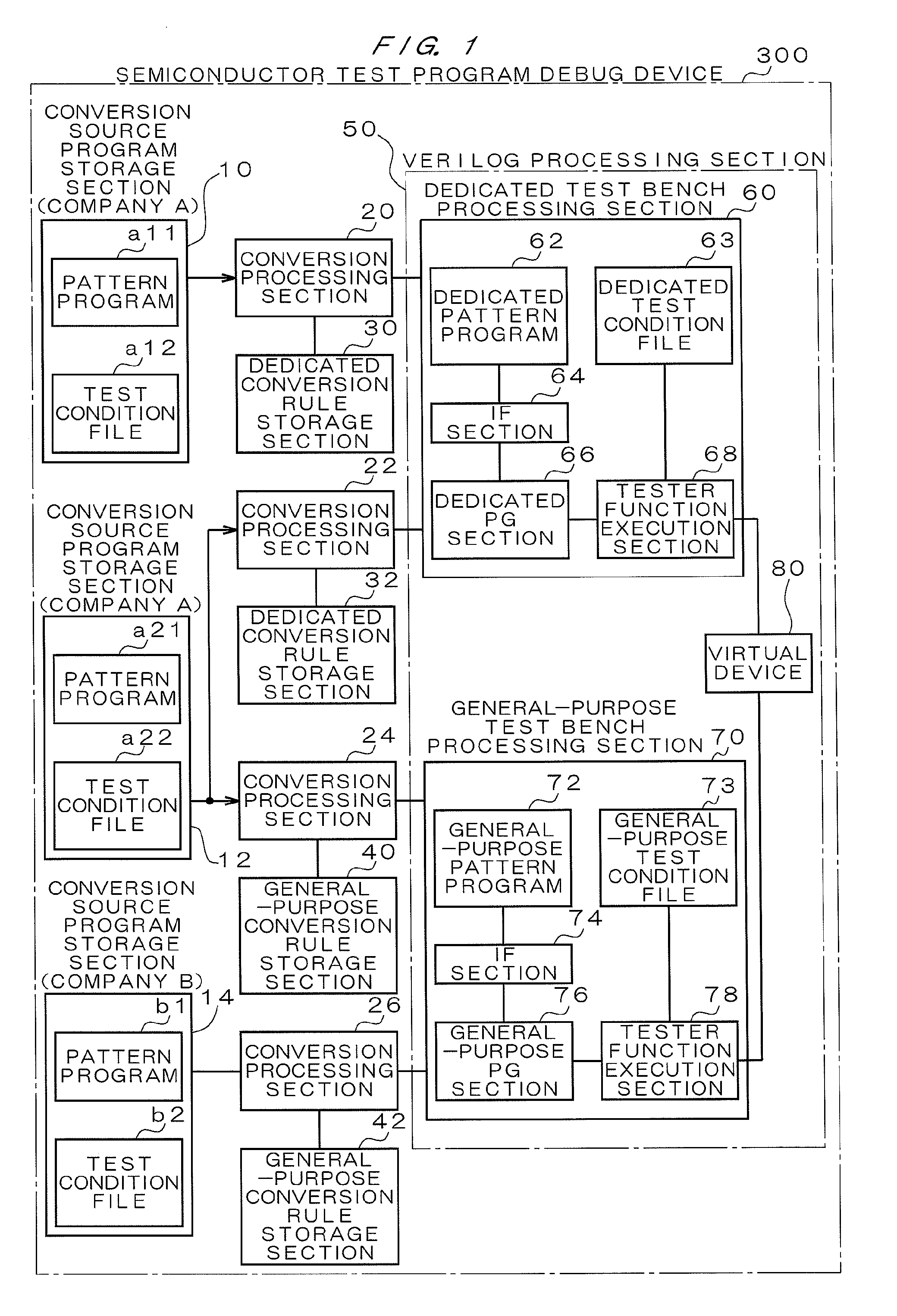
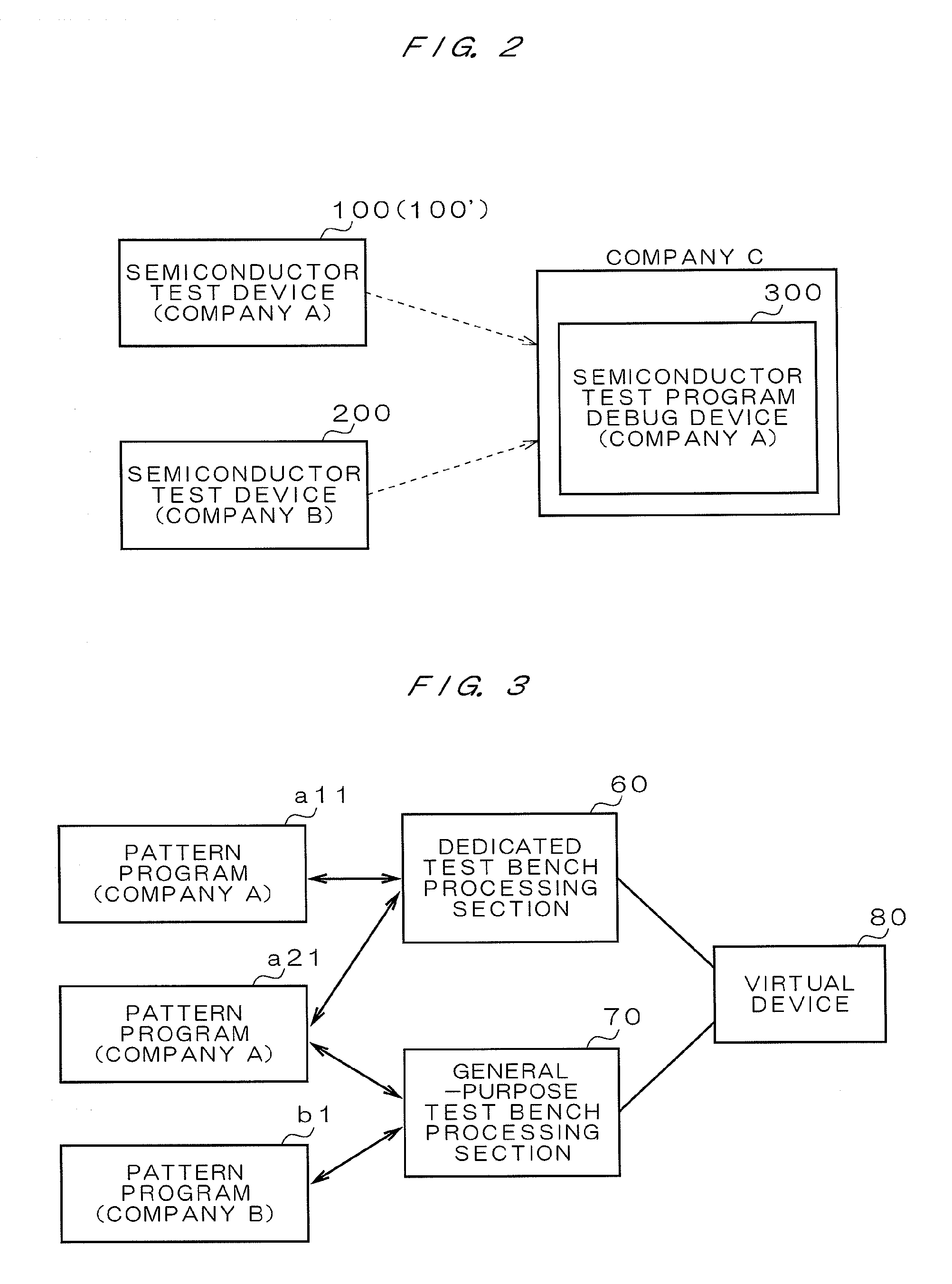
test bench processing unit that generates a pseudo test
signal corresponding to a test signal that is applied to the device under test and also generates a response signal of the virtual device that corresponds to the pseudo test signal; a conversion source program storage unit that stores each of a plurality of the semiconductor test programs that have different specifications; a conversion rule storage unit that stores conversion rules corresponding to each of the plurality of specifications; and a conversion processing unit that, by converting the semiconductor test program that is stored in the conversion source program storage unit using the conversion rule corresponding to specifications of the semiconductor test program that is stored in the conversion rule storage unit, generates the test bench processing unit that corresponds to the semiconductor test program. As a result, even in a case in which there are a plurality of semiconductor test devices or semiconductor test programs that have different specifications, a
virtual test (input and output operations for pseudo test signals and response signals) can be executed with respect to a virtual device in accordance with the respective specifications, and because it is not necessary to provide a semiconductor test program debug device for each specification, unnecessary facilities can be reduced.
[0008]Further, the above described virtual device and test bench processing unit are preferably implemented by the same
hardware description language. More specifically,
Verilog-HDL or
VHDL is preferably used for the aforementioned
hardware description language. It is thereby possible to implement the functions of the test bench processing unit together with a virtual device using
Verilog-HDL or
VHDL as the
hardware description language. In particular, although there are many cases in which a semiconductor test program has specifications that are unique to the manufacturer of a semiconductor test device, since it is possible to convert the semiconductor test program into a test bench processing unit using a general-purpose hardware description language, a semiconductor test program debug device with improved versatility and flexibility can be realized.
[0009]Furthermore, when there are a plurality of semiconductor test devices that are manufactured by different manufacturers and a plurality of semiconductor test programs corresponding to the respective semiconductor test devices, preferably a plurality of specifications have contents that are set for each manufacturer. It is thereby possible to perform debugging of a plurality of semiconductor test programs of different specifications for each manufacturer using a common semiconductor test program debug device.
[0010]In particular, preferably the conversion rules that are stored in the aforementioned conversion rule storage unit and the conversion processing unit are created by manufacturers in correspondence with their respective specifications. It is thereby possible to create a general-purpose test bench unit that operates with a common semiconductor test program debug device without disclosing detailed internal material of respective manufacturers with respect to each manufacturer of competing semiconductor test devices, and to facilitate the common use of the semiconductor test program debug device.
[0012]It is also preferable that, when the test bench processing unit is specified based on the conversion rule, the aforementioned conversion processing unit performs inverse conversion that generates a corresponding semiconductor test program. As a result, reciprocal conversion of semiconductor test programs of different specifications can be carried out through a test bench processing unit that is created temporarily, specifications of semiconductor test programs of respectively different manufacturers or model numbers or versions or the like can be automatically changed, and in addition to effective utilization of semiconductor test programs, errors in specification changes due to manual operations can be prevented.

