

Integrated circuit package and manufacturing method thereof
a technology of integrated circuits and manufacturing methods, applied in the direction of conductive pattern formation, printed circuit non-printed electric components association, semiconductor/solid-state device details, etc., can solve the problems of limited size of solder-halls and bumps, unfavorable increase of the total thickness of the pcb, etc., and achieve the effect of not increasing the thickness and size of the ic packag
- Summary
- Abstract
- Description
- Claims
- Application Information
AI Technical Summary
Benefits of technology
Problems solved by technology
Method used
Image

Examples
Embodiment Construction
[0028]Hereinafter, exemplary embodiments of the present invention will be described with reference to the accompanying drawings. For the purposes of clarity and simplicity, a detailed description of known functions and configurations incorporated herein will be omitted as it may make the subject matter of the present invention unclear.
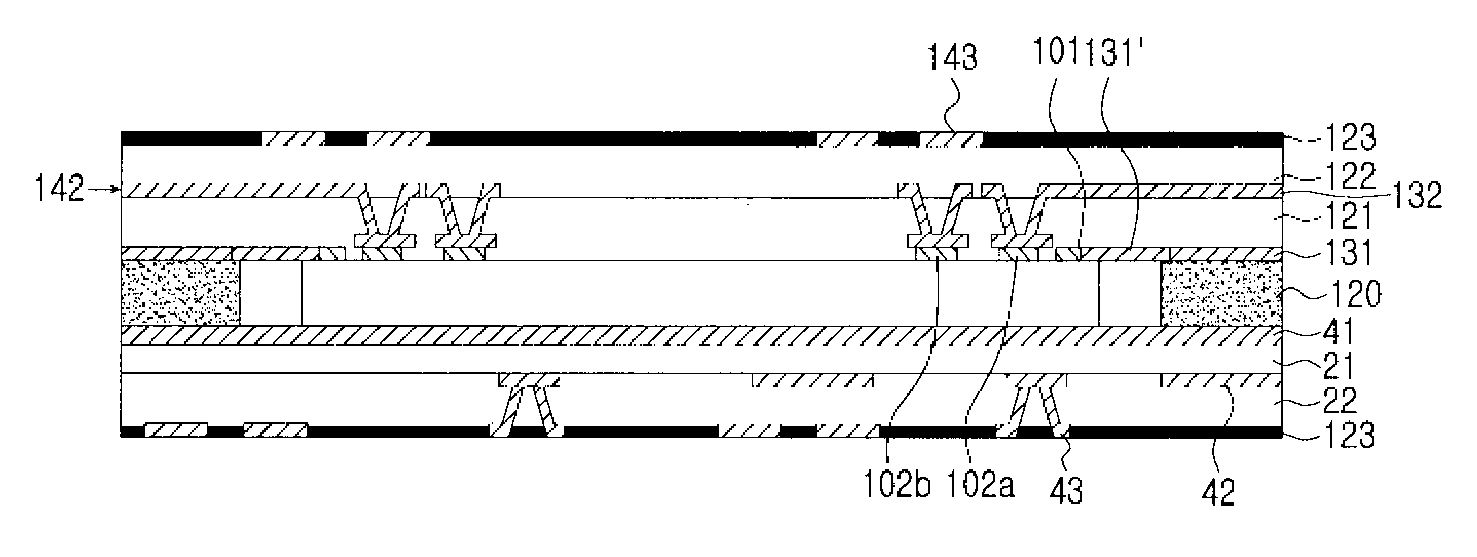
[0029]FIG. 4 is a perspective top view illustrating a part of the fan-out structure in a wafer level package according to an embodiment of the present invention.
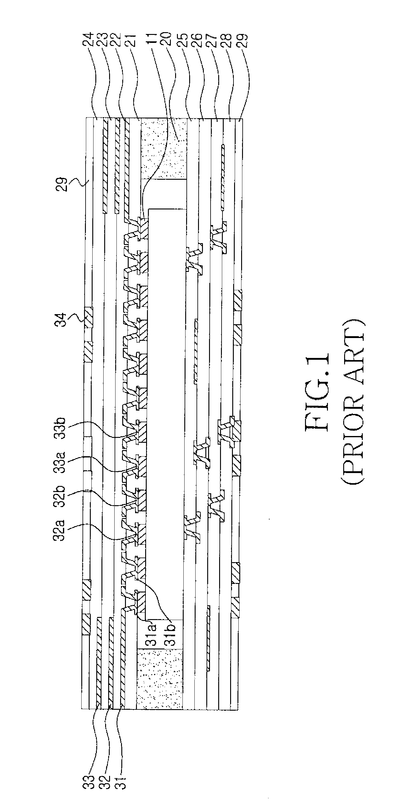
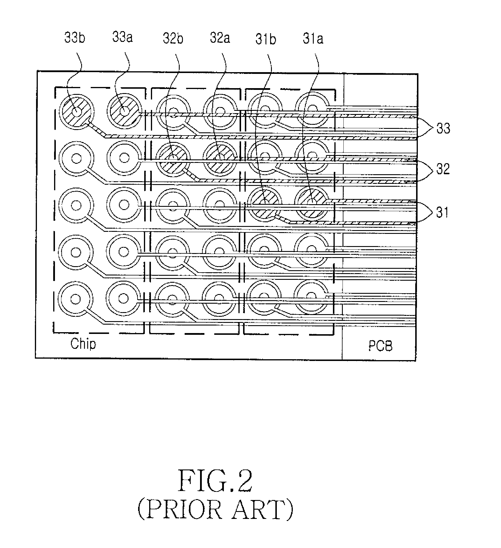
[0030]Referring to FIG. 4, the fan-out structure of the present invention includes solder-ball lands on an IC chip, which are sequentially arranged in an array form from an outermost area. In comparison to the solder-ball lands 132a and 132b arranged at an inner area, the solder-ball lands 131′ in the outermost area are smaller size and have narrower intervals there-between. During the arrangement of the solder-ball lands, the number of the solder-ball arrays can be reduced by initially arrangi...
PUM
| Property | Measurement | Unit |
|---|---|---|
| frequency | aaaaa | aaaaa |
| area | aaaaa | aaaaa |
| size | aaaaa | aaaaa |
Abstract
Description
Claims
Application Information