Charged particle beam lithography apparatus and charged particle beam lithography method

a lithography apparatus and charge technology, applied in photomechanical apparatus, instruments, nuclear engineering, etc., can solve the problems of inefficiency in proximity effect correction calculation and inefficient calculation, and achieve the effect of efficiently performing pattern area density calculation and proximity effect correction calculation

Active Publication Date: 2009-03-05
NUFLARE TECH INC
View PDF6 Cites 21 Cited by
  • Summary
  • Abstract
  • Description
  • Claims
  • Application Information

AI Technical Summary

Benefits of technology

[0012]An object of the present invention is to provide a lithography apparatus and a lithography method capable of performing a pattern area density calculation and a proximity effect correction calculation efficiently.

Problems solved by technology

Thus, there is a problem that calculations cannot be performed efficiently due to variations in calculation time for each block because the number of shots varies from block to block of the same size.
Therefore, there is a problem that if the block size is made non-uniform for the calculation of pattern area density, the proximity effect correction calculation cannot be performed efficiently due to variations in calculation time for each block.
Thus, giving priority to one results in a problem for the other.

Method used


Image

  • Charged particle beam lithography apparatus and charged particle beam lithography method
  • Charged particle beam lithography apparatus and charged particle beam lithography method
  • Charged particle beam lithography apparatus and charged particle beam lithography method

Examples


first embodiment

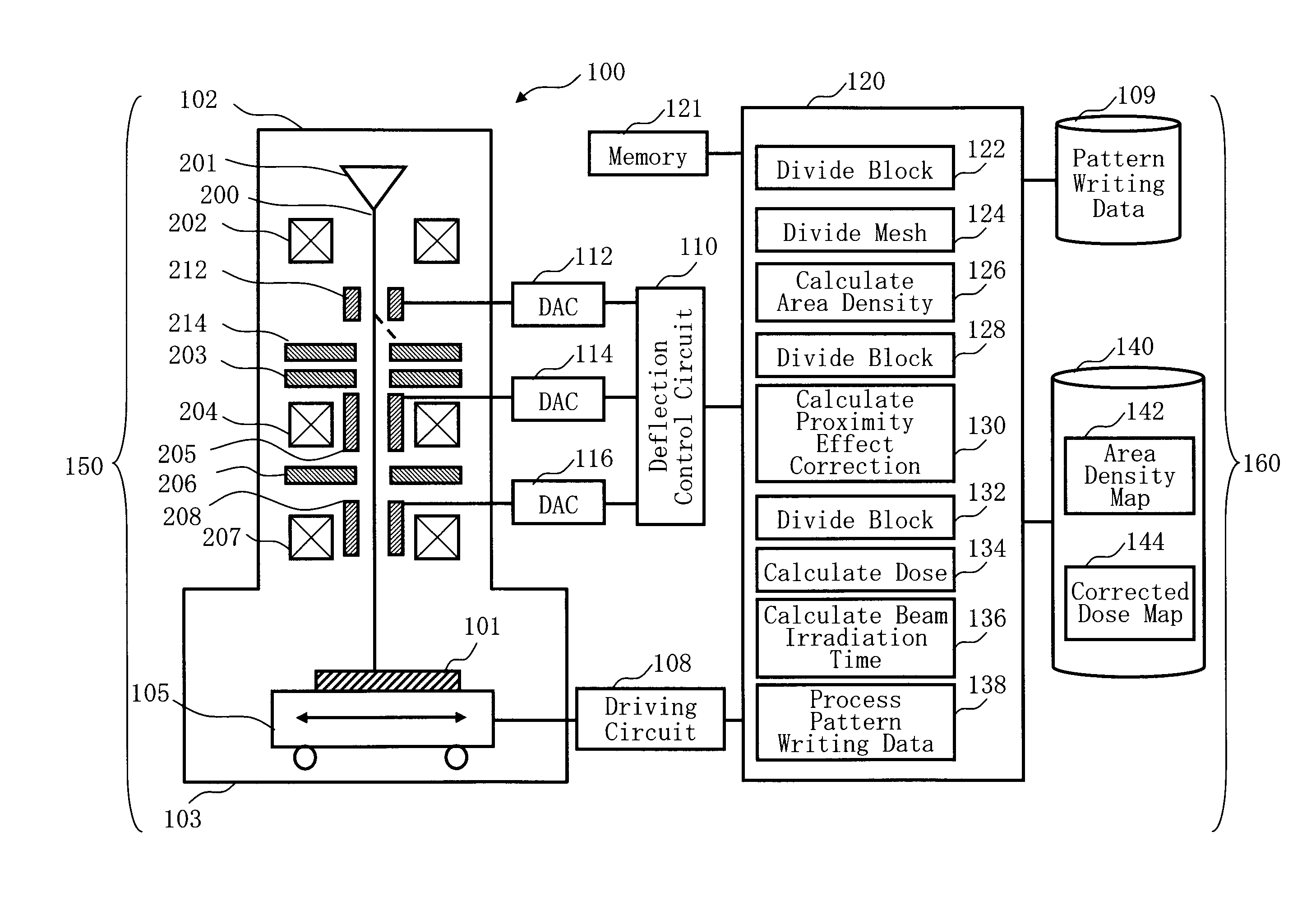
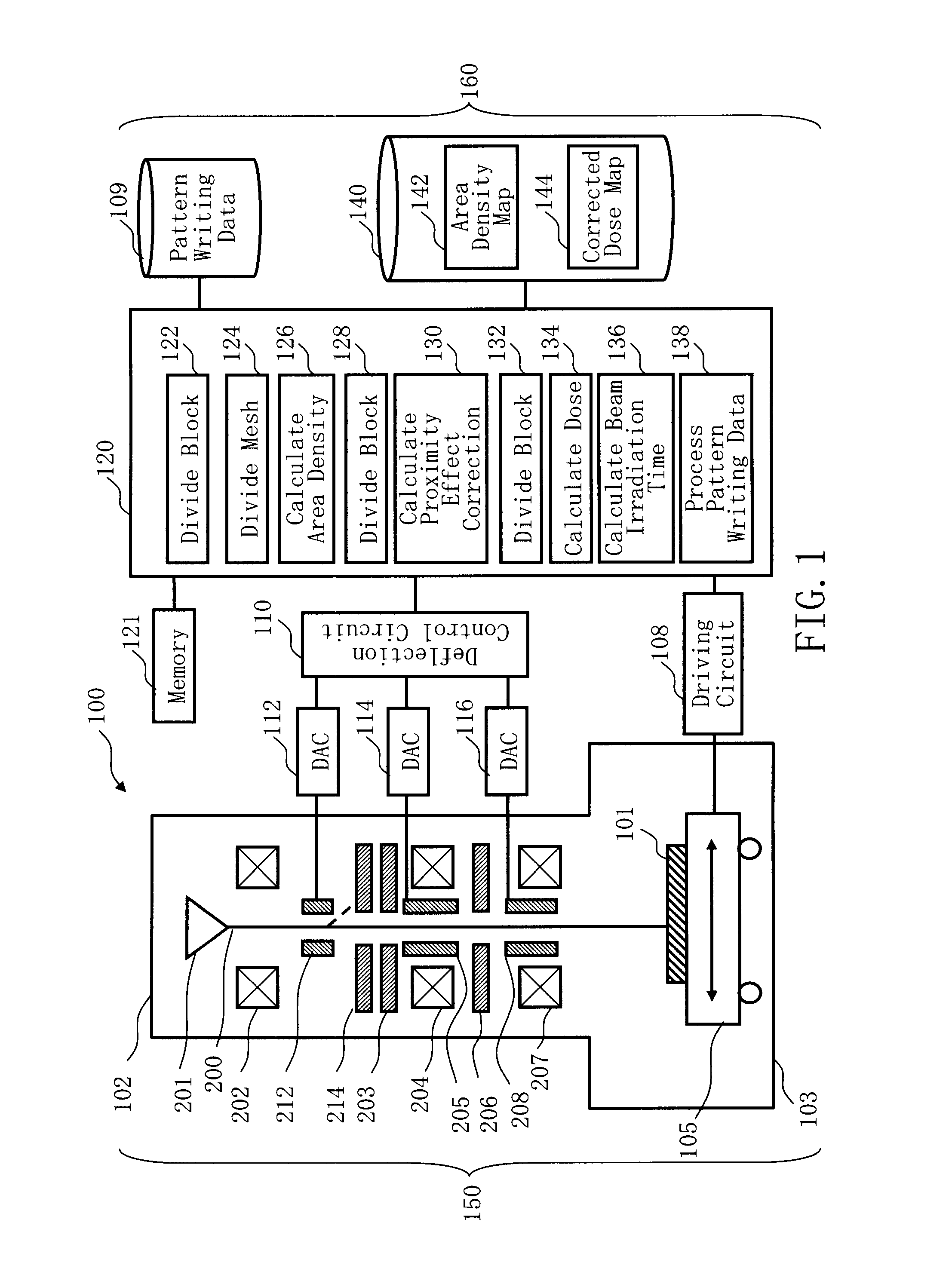
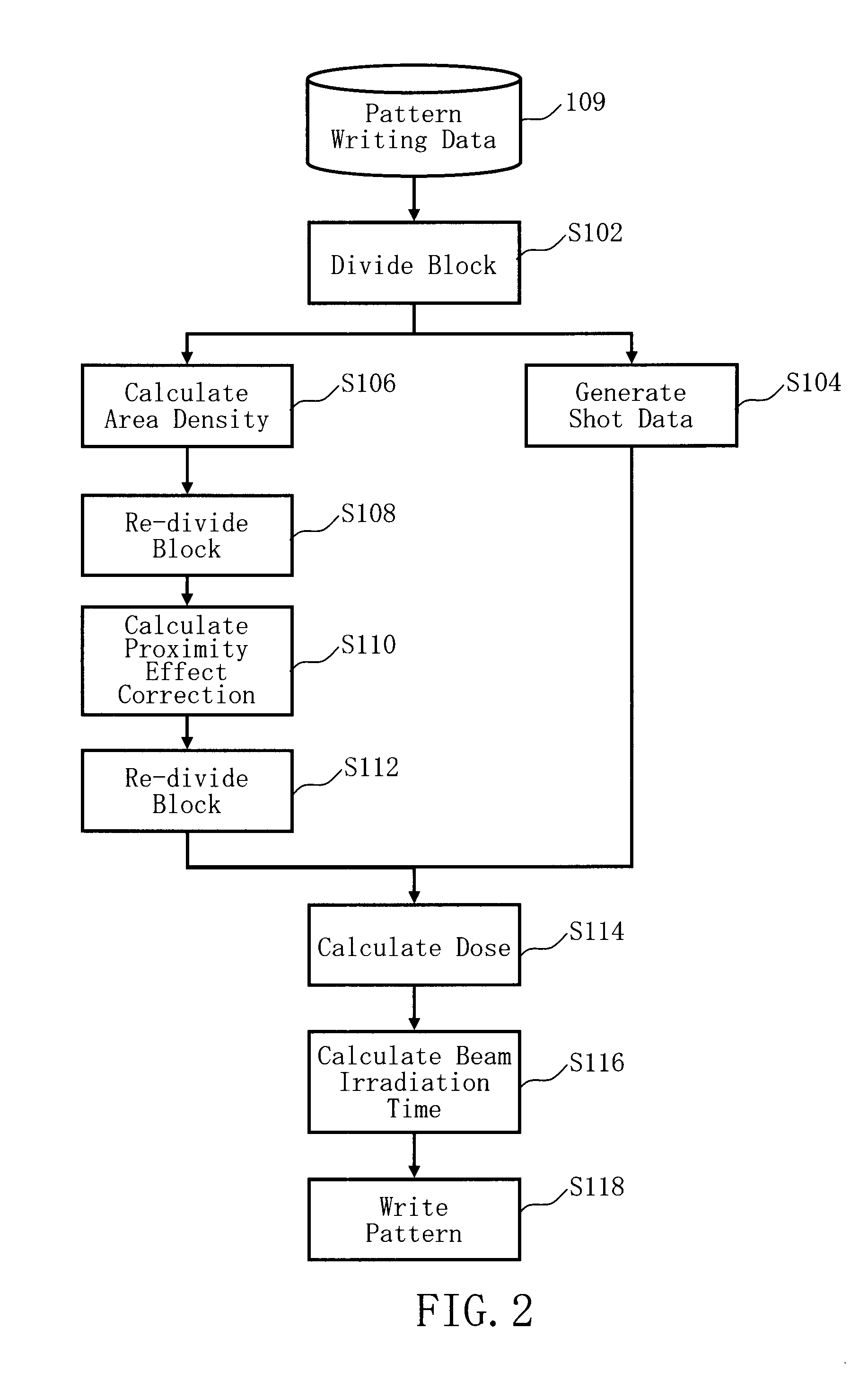
[0023]FIG. 1 is a conceptual diagram showing the configuration of a writing apparatus in the first embodiment. In FIG. 1, a writing apparatus 100 includes a writing unit 150, which is an example of pattern generator, and a controller 160. The writing apparatus 100 is an example of charged particle beam lithography apparatus. Then, the writing apparatus 100 forms (or “writes” or “draws”) a desired pattern on a target object 101 (or “target workpiece 101”) by using EB lithography technique. The pattern writing unit 150 has an electron lens barrel 102 and a pattern writing chamber 103. In the electron lens barrel 102, an electron gun assembly 201, an illumination lens 202, a blanking (BLK) deflector 212, a blanking (BLK) aperture plate 214, a first aperture plate 203, a projection lens 204, a deflector 205, a second aperture plate 206, an objective lens 207, and a deflector 208 are arranged. An XY stage 105 movably arranged is arranged inside the pattern writing chamber 103. The target...


PUM


Abstract

A charged particle beam lithography apparatus includes a first block area divider configured to divide a pattern forming area into a plurality of first block areas in order to make a number of shots when forming a pattern substantially equal; an area density calculator configured to calculate, using a plurality of small areas obtained by virtually dividing the pattern forming area into mesh areas of a predetermined size smaller than all of the first block areas, a pattern area density of each small area positioned therein for each of the first block areas; a second block area divider configured to re-divide the pattern forming area divided into the plurality of first block areas into a plurality of second block areas of a uniform size, which is larger than the small area; a corrected dose calculator configured to calculate, using the pattern area density of each small area, a proximity effect-corrected dose in each corresponding small area positioned inside the second block area for each of the second block areas; a beam dose calculator configured to calculate, using the proximity effect-corrected dose of each small area, a beam dose of a charged particle beam in each corresponding small area; and a pattern generator configured to form a predetermined pattern on a target object by irradiating a charged particle beam of the beam dose calculated for each of the small areas.

Description

CROSS-REFERENCE TO RELATED APPLICATION[0001]This application is based upon and claims the benefit of priority from prior Japanese Patent Application No. 2007-229853 filed on Sep. 5, 2007 in Japan, the entire contents of which are incorporated herein by reference.BACKGROUND OF THE INVENTION[0002]1. Field of the Invention[0003]The present invention relates to a charged particle beam lithography apparatus and a charged particle beam lithography method and, for example, relates to a charged particle beam writing apparatus and a charged particle beam writing method for correcting dimension variations due to a proximity effect.[0004]2. Related Art[0005]Lithography technology in charge of development of more microscopic semiconductor devices is an extremely important process among semiconductor manufacturing processes that solely generates patterns. In recent years, with increasingly higher integration of LSI, a circuit linewidth demanded for semiconductor devices is becoming finer year af...

Claims


Application Information

Patent Timeline
Patent Type & Authority Applications(United States)
IPC IPC(8): G21K5/00
CPCB82Y10/00H01J37/3174H01J37/3026B82Y40/00G03F7/2059Y10S430/143
Inventor OOGI, SUSUMUHIGURASHI, HITOSHIANPO, AKIHITOYAMAMOTO, TOSHIRO
Owner NUFLARE TECH INC
Why Eureka
Try Eureka