Check patentability & draft patents in minutes with Patsnap Eureka AI!

Receiver circuit for use in a semiconductor integrated circuit

Inactive Publication Date: 2009-03-05
SK HYNIX INC
View PDF9 Cites 6 Cited by
  • Summary
  • Abstract
  • Description
  • Claims
  • Application Information

AI Technical Summary

Benefits of technology

[0010]Receiver circuits that require less area and h

Problems solved by technology

As transmission speeds increase it becomes more difficult to ensure a sufficient sensing margin.
Further, attenuation, such as Inter-Symbol Interference (ISI), of received signals can make it difficult for the receiver to accurately sense the signals.
Unfortunately, circuit implementation of such solutions can be complicated and can occupy a large area, limiting integration.
Further, in case of the FFE method, noise components of a signal may be amplified.

Method used


Image

  • Receiver circuit for use in a semiconductor integrated circuit
  • Receiver circuit for use in a semiconductor integrated circuit
  • Receiver circuit for use in a semiconductor integrated circuit

Examples


Embodiment Construction

.”

BRIEF DESCRIPTION OF THE DRAWINGS

[0013]Features, aspects, and embodiments are described in conjunction with the attached drawings, in which:

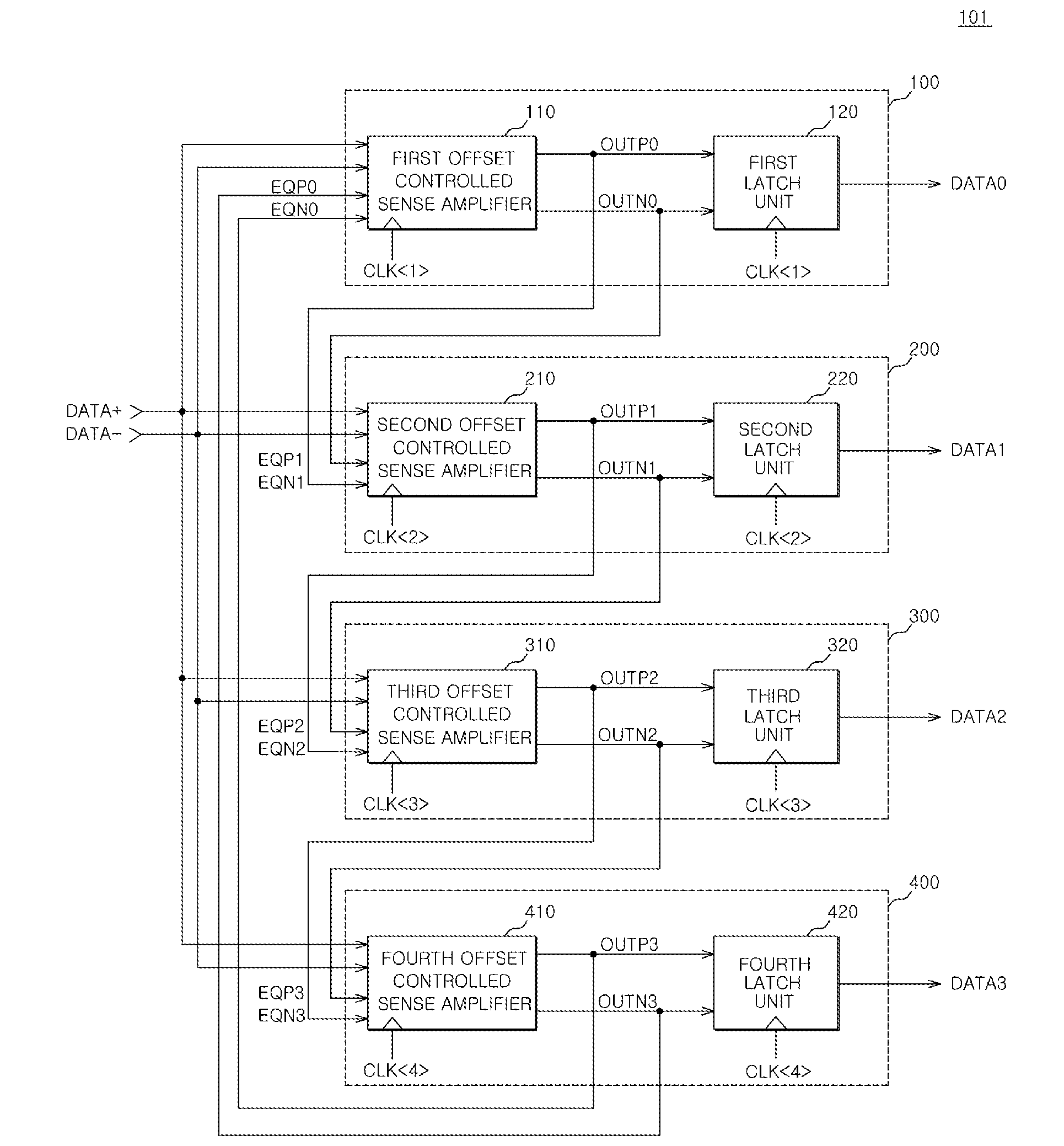
[0014]FIG. 1 is a block diagram of a receiver circuit according to an embodiment described herein.

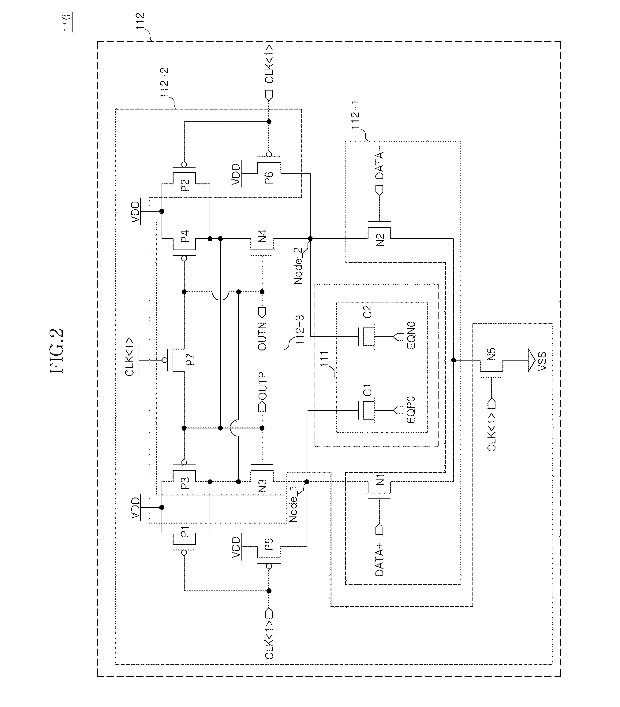
[0015]FIG. 2 is a detailed circuit diagram of a first offset controlled sense amplifier that can be included in the diagram illustrated in FIG. 1.

[0016]FIG. 3A is a drawing illustrating a waveform of an output signal of a conventional receiver circuit.

[0017]FIG. 3B is a drawing illustrating a waveform of an output signal of the receiver circuit which can be included in the diagram illustrated in FIG. 1.

DETAILED DESCRIPTION

[0018]FIG. 1 is a block diagram of a receiver circuit 101 according to an embodiment described herein. Referring to FIG. 1, the receiver circuit 101 can include first to fourth phase transmitters 100, 200, 300, and 400. The first phase transmitter 100 can include a first offset controlled sense amplifier 110 and a first latch uni...


PUM


Abstract

A receiver circuit for sensing and transmitting input data in sync with a plurality of clock signals having mutually different phase sequentially enabled comprising a sense amplifier configured to receive, as offset voltages, first signals which can be obtained by amplifying the input data in sync with a first clock signal of the plurality of clock signals, being driven in sync with a second clock signal enabled subsequently to the first clock signal, and outputting second signals, and a discharging controller configured to control a discharging speed of the sense amplifier according to the offset voltages to control a driven speed of the sense amplifier.

Description

CROSS REFERENCE TO RELATED APPLICATIONS[0001]The present application claims priority under 35 U.S.C. 119(a) to Korean application number 10-2007-0089474, filed on Sep. 4, 2007, in the Korean Intellectual Property Office, the disclosure of which is incorporated herein in its entirety by reference, as if set forth in full.BACKGROUND[0002]1. Technical Field[0003]The embodiments described herein relate to semiconductor integrated circuits, and in particular, to a receiver circuit for a semiconductor integrated circuit.[0004]2. Related Art[0005]The need for low-power supply voltage capability and high-speed interfaces is becoming more prevalent for conventional semiconductor integrated circuits as the operational speeds of such circuits increases.[0006]Input receivers within such conventional semiconductor integrated circuits, such as semiconductor memories, are configured to buffer external signals and to transfer the signals to internal circuits and systems. The buffering operation oft...

Claims


Application Information

Patent Timeline
IPC IPC(8): H03L7/00
CPCH04L7/0337H04B1/06H04L7/00
Inventor OH, IC SUPARK, KUN WOOKIM, YONG JUSONG, HEE WOONGKIM, HYUNG SOOHWANG, TAE JINCHOI, HAE RANGLEE, JI WANG
Owner SK HYNIX INC
Features
  • R&D
  • Intellectual Property
  • Life Sciences
  • Materials
  • Tech Scout
  • Unparalleled Data Quality
  • Higher Quality Content
  • 60% Fewer Hallucinations
Learn More