Electronic shielding apparatus and methods

Inactive Publication Date: 2009-03-12
AUTOSPLICE SYST +1
View PDF32 Cites 37 Cited by
  • Summary
  • Abstract
  • Description
  • Claims
  • Application Information

AI Technical Summary

Benefits of technology

[0024]In a fifth aspect of the invention, a method of manufacturing a shielded electronic component is disclosed. In one embodiment, the method comprises: disposing a shield structure formed at least partly via a selective metal deposition process in proximity with and at least partially surrounding an electronic component; placing said electronic component and said shield structure in a mold; and encapsulating said electronic component and said shield structure so as to form a unitary assembly. In one variant, said electronic component comprises an integrated circuit, and said shield structure is electroformed and adapted to substantially mitigate noise in the range of 2-6 GHz.
[0025]In a sixth aspect of the invention, a

Problems solved by technology

However, these emissions represent a significant source of possible interference with the operation of the components or the device at large, and hence are of significant concern.
However, each of the foregoing methods suffers from one or more disabilities, including inter alia: (i) adding substantially to the cost of the shielded device, (ii) having limits in terms of durability, minimum size and area consumed, cost of manufacturing, and even aesthetics, (iii) d

Method used


Image

  • Electronic shielding apparatus and methods
  • Electronic shielding apparatus and methods
  • Electronic shielding apparatus and methods

Examples


first embodiment

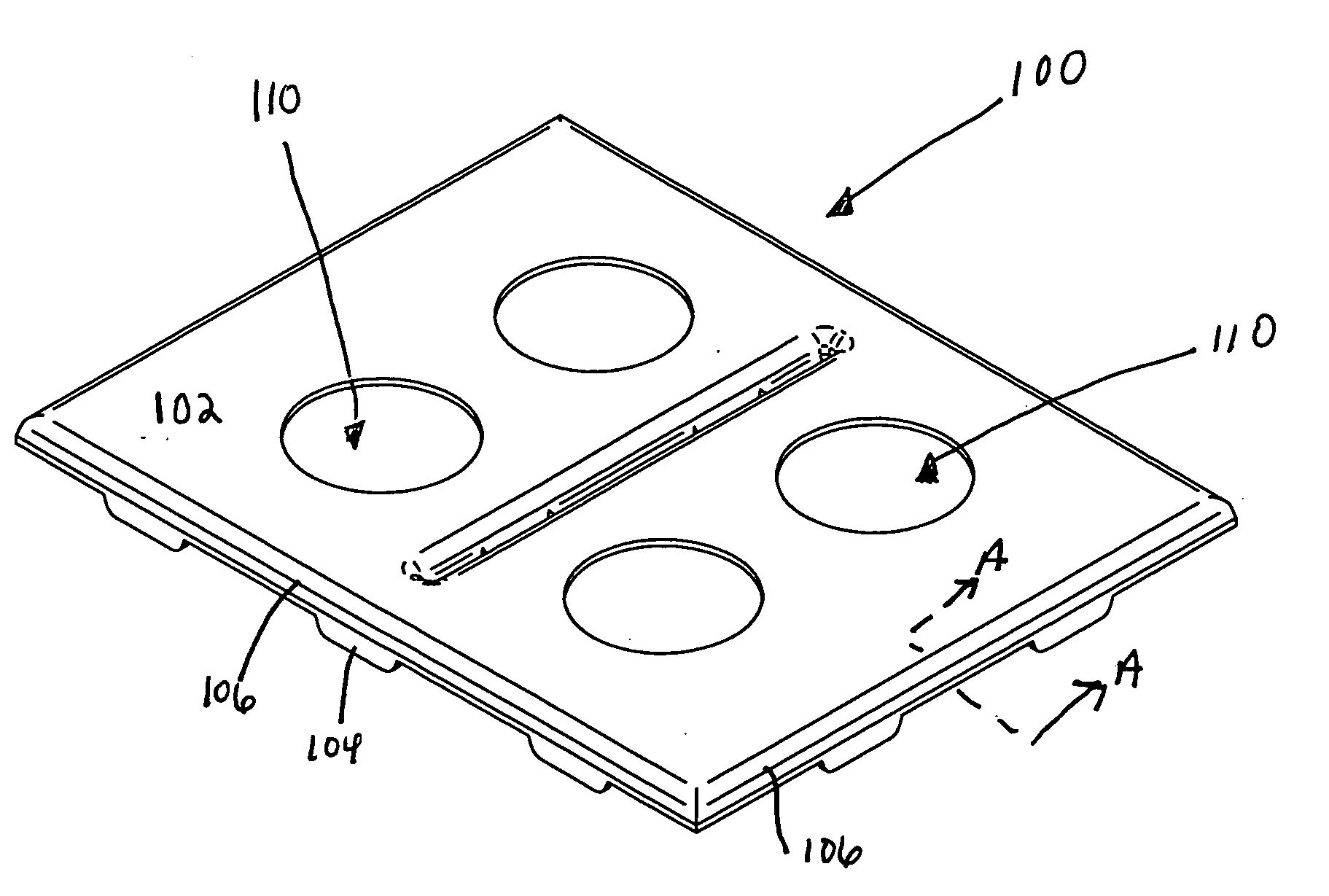
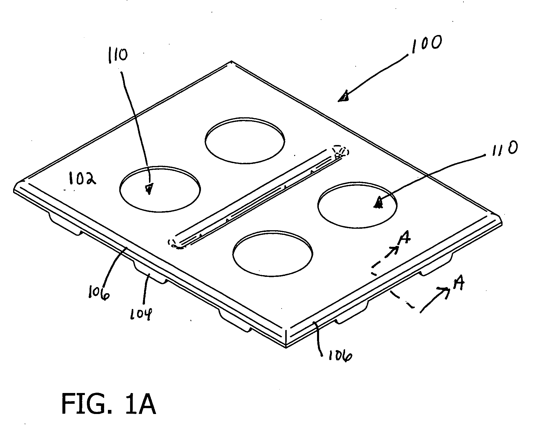
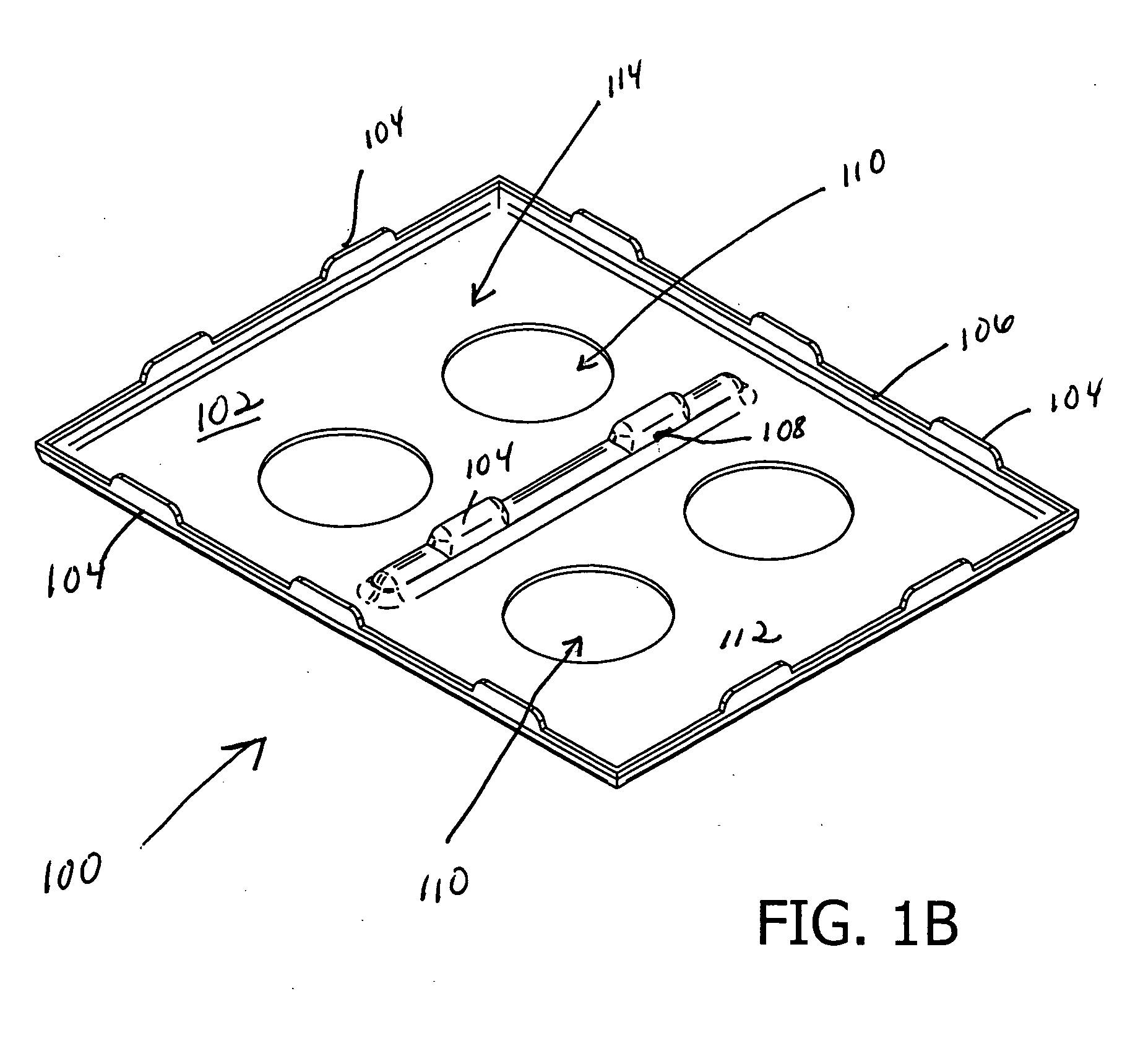
[0075]FIGS. 1A and 1B illustrate an integrated shield structure 100 manufactured in accordance with the principles of the present invention. The integrated shield structure 100, in one or more embodiments, comprises an electroformed copper or nickel based alloy structure suitable for attenuating spurious electromagnetic or other noise or undesired signals. Specifically, in one embodiment, the integrated shield structure 100 is adapted to attenuate spurious electromagnetic noise in the 2-6 GHz frequency range, however various levels of attenuation and response as a function of frequency can be achieved via adaptation of various features of the integrated shield structure 100 of FIGS. 1A and 1B described herein, such adaptation being well within the skill of the ordinary artisan given the present disclosure.

[0076]The exemplary electroforming process comprises a process of precision metal part fabrication which uses electro-deposition in a plating bath over a precise base form or “mand...

second embodiment

[0120]FIG. 7A illustrates a carrier tape 702, in which a shield structure array 400 resides. Similar to the carrier shown in FIG. 7, the shield structure array 400 can be removed from the cavity within the carrier tape 702 via a nozzle and subsequently be placed over an electronic component prior to subsequent manufacturing processes such as encapsulation and the like.

[0121]Referring now to FIGS. 8A-8D, additional embodiments of shield structures 800 according to the invention are shown and described in detail.

[0122]As can be seen in FIG. 8A, the shield structure comprises an electroformed or chemically etched base material 802 characterized by fill features 810, a cavity dividing wall 808 and an external wall 806. The profile of the integrated shield structure 800 of FIG. 8A comprises a curved profile, while the dividing wall 808 can be formed into an irregular pathway. This illustrates the advantages of the electroforming or chemical milling processes as it applies to more complex...


PUM


Abstract

A shielding apparatus useful in the attenuation of electronic noise or spurious electric signals is disclosed. In one embodiment, the shielding apparatus is encapsulated with an electronic component such as an integrated circuit. At least parts of the apparatus are formed using a selective metal deposition process (e.g., electroforming) that increases manufacturing efficiency and provides enhanced mechanical and structural features, as well as reduced cost. In another embodiment, the shielding apparatus comprises an array. Methods of manufacturing and utilizing the shielding apparatus are also disclosed.

Description

COPYRIGHT[0001]A portion of the disclosure of this patent document contains material that is subject to copyright protection. The copyright owner has no objection to the facsimile reproduction by anyone of the patent document or the patent disclosure, as it appears in the Patent and Trademark Office patent files or records, but otherwise reserves all copyright rights whatsoever.1. FIELD OF THE INVENTION[0002]The present invention relates to the field of electrical devices and electronics, and specifically in one embodiment to methods for reducing the effects of spurious electrical signals on electronic components.2. DESCRIPTION OF RELATED TECHNOLOGY[0003]In electronic devices such as e.g., cellular telephones and other wireless applications, it is often necessary to shield the printed circuit board and / or other electronic components to limit or prevent emissions caused or received by such components. These “spurious” signals (typically radio frequency or electromagnetic energy of a ...

Claims


Application Information

Patent Timeline
IPC IPC(8): H05K9/00C25D5/02
CPCH01L23/552H01L23/66H01L2924/3025H01L2924/16251H01L2924/16153H01L2224/73265H01L2224/48227H01L25/16H01L2924/09701H01L2924/1616H01L2924/19105H05K9/003H01L2224/32225H01L2924/00012H01L2924/00H01L24/73H01L2924/14
Inventor BOGURSKY, ROBERTKRONE, KENNETHGRABAU, FREDERICK W.BELLANTONI, PETERSAUNDERS, MARK
Owner AUTOSPLICE SYST
Why Eureka
Try Eureka