Acceleration sensor device

a sensor device and acceleration technology, applied in the direction of measurement devices, speed/acceleration/shock measurement, instruments, etc., can solve the problems of large offset voltage and flexible arms to be broken, and achieve the effect of reducing offset voltage, reducing damping period of oscillation, and facilitating transmission

Inactive Publication Date: 2009-03-19
HITACHI METALS LTD
View PDF8 Cites 6 Cited by
  • Summary
  • Abstract
  • Description
  • Claims
  • Application Information

AI Technical Summary

Benefits of technology

[0023]In an acceleration sensor device according to the present invention, an upper regulation plate protrudes from outside walls of a support frame of an acceleration sensor chi to partition the space accommodating the acceleration sensor chip in a protection case by the protrusion and to prevent air circulation above and below the upper regulation plate. Therefore, a temperature rise, due to an IC circuit, between the piezo-resistors disposed adjacent to a mass portion and the piezo-resistors disposed adjacent to a support frame on the top surface of a flexible arm can be kept uniform to reduce offset voltage. Moreover, the upper regulation plate causes damping effect to reduce the damping period of oscillation for rapid acceleration changes. Further, when chipping occurs in a silicon substrate forming the upper regulation plate, since the upper regulation plate is larger than the acceleration sensor chip, the chips from the silicon substrate are seldom involved in the sensor. Moreover, the gap between a side of the upper regulation plate and an inside wall of the protection case is small and, furthermore, the upper regulation plate and the protection case are joined by lead wires. Thus, it is also expected that the heat of the upper regulation plate can easily be transmitted to the protection case and released.

Problems solved by technology

The fact that small acceleration can be detected has caused flexible arms to be broken because great impact makes the amplitude of a mass portion too large.
Specifically, there has been a problem that offset voltage is large.

Method used


Image

  • Acceleration sensor device
  • Acceleration sensor device
  • Acceleration sensor device

Examples


example 1

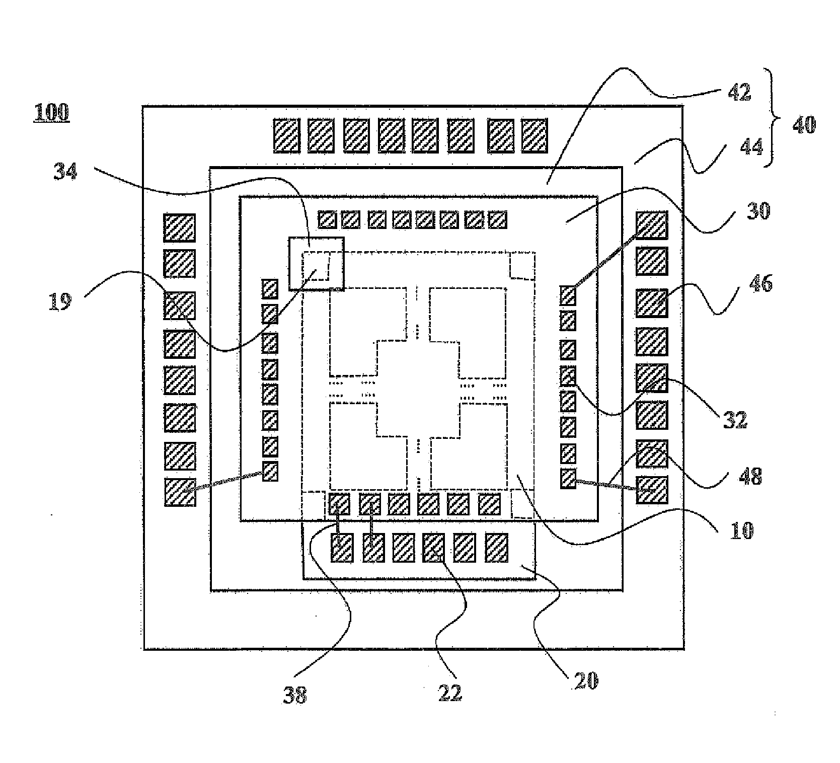
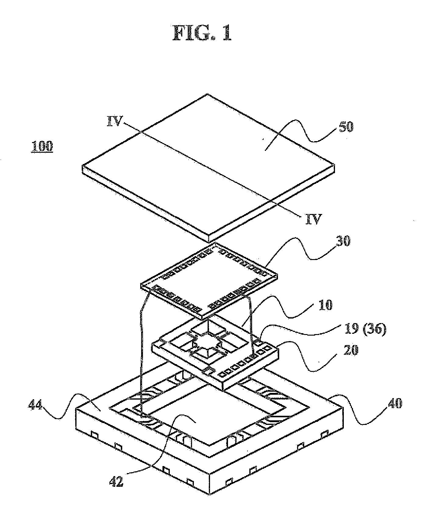
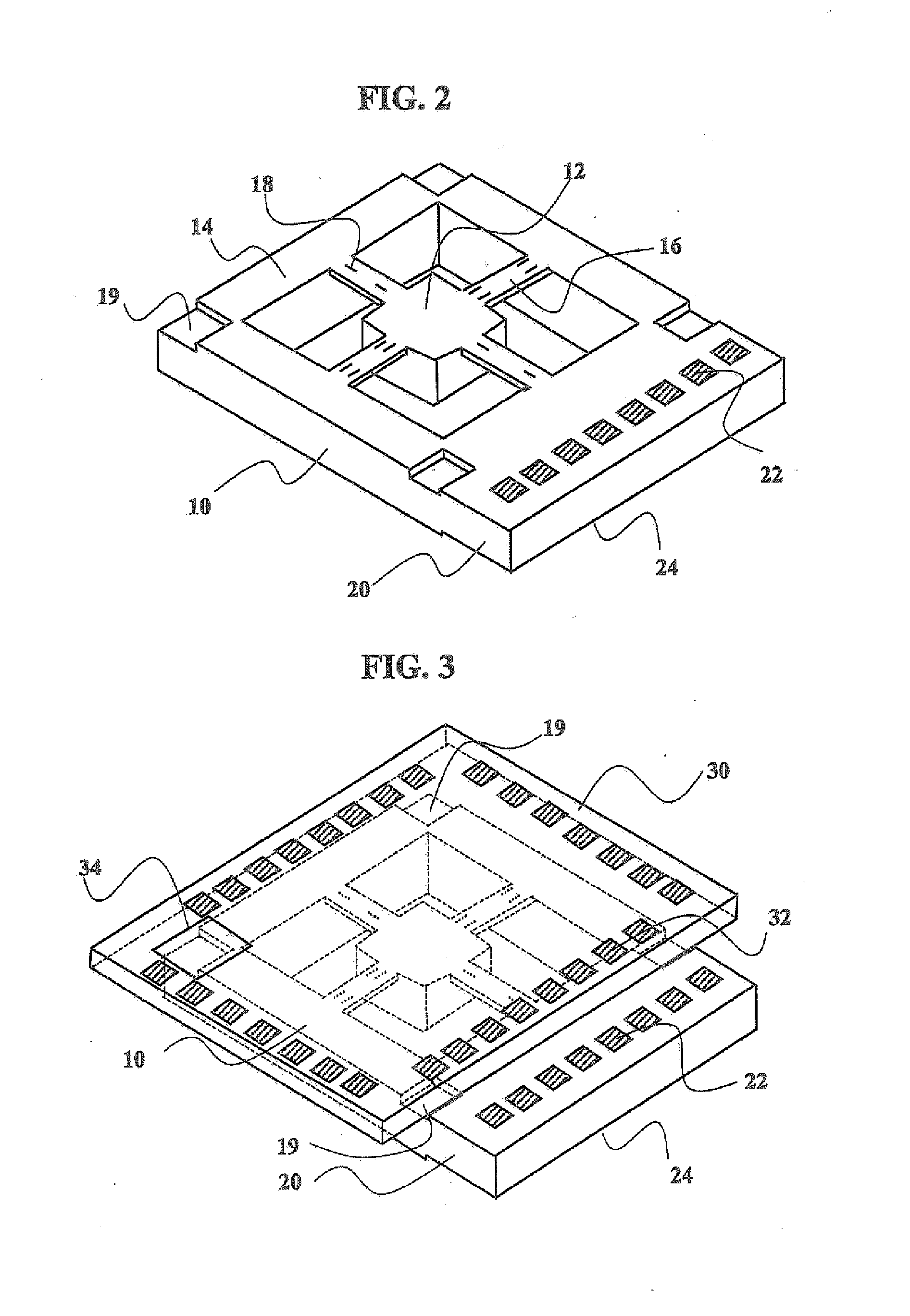
[0048]An acceleration sensor device of EXAMPLE 1 according to the present invention will be described with FIG. 1 to FIG. 5. FIG. 1 is an exploded perspective view of the acceleration sensor device of EXAMPLE 1; FIG. 2 is a perspective view showing an acceleration sensor chip used in the acceleration sensor device of EXAMPLE 1; FIG. 3 is a perspective view of the acceleration sensor chip with an upper regulation plate mounted thereon; FIG. 4 is a cross-sectional view taken along a line IV-IV of FIG. 1; and FIG. 5 is a plan view showing the acceleration sensor device of FIG. 1 with a lid removed. In the acceleration sensor device 100 of EXAMPLE 1, the upper regulation plate 30 with its circuit mounting surface on the top is bonded to the top surface of the acceleration sensor chip 10 by mixed and kneaded adhesive 36 containing about 10 wt % of rigid plastic balls (20 μm in diameter) and the acceleration sensor chip 10 is inserted and bonded in a protection case 40. To bond the accele...

example 2

[0066]The relationship between the offset voltage and the distance ratio was measured by using an acceleration sensor device according to the present invention, in which the size of the upper regulation plate is changed, and the ratio of the gap, between an inside wall of the protection case and a side of the upper regulation plate, to the gap, between the inside wall of the protection case and an outside wall of the support frame, is changed. Acceleration sensor devices used herein are the same as that of EXAMPLE 1 except for the sizes of the upper regulation plates. In the upper regulation plates, L of the size of 2200 μm in width×L μm in length×200 μm thickness was changed from 1900 μm up to 2800 μm. The upper regulation plate protrudes by 300 μm from the outside wall of the support frame on the side opposite to the side on which the terminal board is disposed because the upper regulation plate is bonded on the acceleration sensor chip so that on the side, of the acceleration sen...

example 3

[0067]The relationship between a location of the temperature sensor disposed on the upper regulation plate and the offset voltage was considered. Acceleration sensor devices used herein have the constitution as described in EXAMPLE 1, and the temperature sensor 34 is disposed on the upper regulation plate corresponding to one of the locations where the upper regulation plate is bonded at the four corners of the support frame. When the center of a temperature measuring portion (size of 300 μm×300 μm) of the temperature sensor 34 was changed in a to-and-fro direction by a distance of W1 and in a right-and-left direction by a distance of W2 up to 300 μm as shown in FIG. 7 from the center of the corner 19 having a recess with the size of 180 μM×180 μm containing adhesive, the offset voltage was measured, and the distribution of the offset voltage is shown in FIG. 8. As seen from FIG. 8, when the center of the temperature measuring portion of the temperature sensor is an area within ±50 ...


PUM


Abstract

An acceleration sensor device comprising: an acceleration sensor chip comprising a mass portion, a support frame and flexible arms having piezo-resistors on their top surfaces; and an upper regulation plate having an IC circuit, which is larger in area than the support frame, bonded to a top surface of the support frame; wherein the acceleration sensor chip and the upper regulation plate are placed in a protection case with a lid. The regulation plate protrudes from outside walls of the support frame to partition the space accommodating the chip in the protection case by the protrusion and to prevent air circulation above and below the regulation plate, so that a temperature rise due to the IC circuit among the piezo-resistors provided on the top surfaces of the flexible arms is kept uniform to reduce offset voltage.

Description

TECHNICAL FIELD[0001]The present invention relates to acceleration sensor devices for detecting acceleration, which are used for toys, automobiles, airplanes, portable terminal devices, and the like, and in particular to an acceleration sensor device which can be manufactured by using semiconductor technology.BACKGROUND ART[0002]Acceleration sensors utilizing physical quantity change such as piezo-resistance effect or capacitance change have been developed and commercialized. Although these acceleration sensors can be widely used in various fields, there has recently been a demand for a smaller acceleration sensor capable of highly sensitively detecting acceleration in multi-axial directions at the same time.[0003]Silicon single crystals have features: they can be an ideal elastic body because of their extremely few lattice defects, they can utilize semiconductor process technology without modification, and the like. Thus, particular attention is paid to semiconductor acceleration s...

Claims


Application Information

Patent Timeline
Patent Type & Authority Applications(United States)
IPC IPC(8): G01P15/12G01P15/18
CPCG01P1/023G01P15/18G01P15/123G01P2015/084G01P15/08G01P15/09
Inventor SAKAGUCHI, ISAO
Owner HITACHI METALS LTD
Why Eureka
Try Eureka