Semiconductor integrated circuit

Active Publication Date: 2009-03-19
SONY CORP
View PDF9 Cites 7 Cited by
  • Summary
  • Abstract
  • Description
  • Claims
  • Application Information

AI Technical Summary

Benefits of technology

[0040]According to the embodiment of the present invention, in moving a switch or changing the number of switches, it suffices principally to change constituent elements other than the voltage line segment of the switch block. Therefore benefits are obtained in that it is easy to make a design change and it is easy to optimize the position and the number of switches. More specifically, in a case where a power supply voltage supply line or a reference voltage supp

Problems solved by technology

This results in a disadvantage of an increase in leakage current via the switch transistor in a state in which the internal circuit is stopped.
However, when a stop period is long, unnecessary power consumption due to an increase in the size of the switch transistor or the number of switch transistors may not be ignored.
Howev

Method used


Image

  • Semiconductor integrated circuit
  • Semiconductor integrated circuit
  • Semiconductor integrated circuit

Examples


Embodiment Construction

[0056]Preferred embodiments of the present invention will hereinafter be described with reference to the drawings.

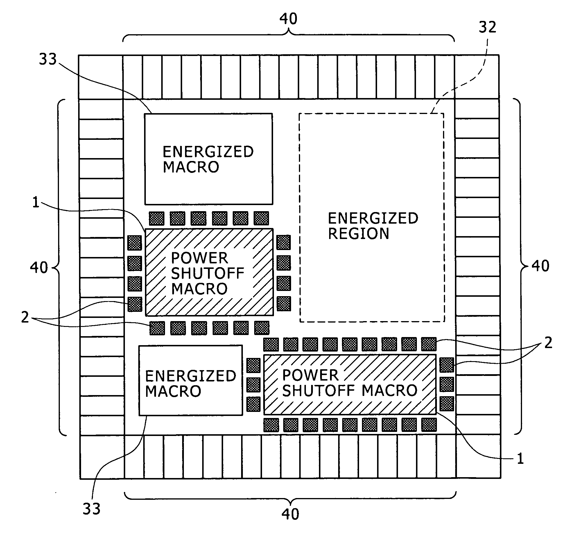
[0057]FIG. 1 shows a general configuration of a semiconductor integrated circuit according to an embodiment of the present invention.

[0058]In FIG. 1, a plurality of input-output cells 40 are respectively arranged so as to form a column along four sides of a rectangular semiconductor chip on which the semiconductor integrated circuit is formed.

[0059]A few circuit blocks are arranged in a chip area for circuit arrangement which area is surrounded on all four sides by the input-output cells 40 shown in FIG. 1. In the example shown in FIG. 1, a basic configuration of the semiconductor integrated circuit which configuration is referred to as an “energized region,” for example an energized circuit block 32 including a CPU, a register, a memory, a power supply circuit and the like is disposed in the chip area. The energized circuit block 32 corresponds to a circuit block to whi...


PUM


Abstract

A semiconductor integrated circuit including: a circuit block having an internal voltage line; an annular rail line forming a closed annular line around the circuit block and supplied with one of a power supply voltage and a reference voltage; and a plurality of switch blocks arranged around the circuit block along the annular rail line, the plurality of switch blocks each including a voltage line segment forming a part of the annular rail line and a switch for controlling connection and disconnection between the voltage line segment and the internal voltage line.

Description

CROSS REFERENCES TO RELATED APPLICATIONS[0001]The present invention contains subject matter related to Japanese Patent Application JP 2007-241517 filed in the Japan Patent Office on Sep. 18, 2007, the entire contents of which being incorporated herein by reference.BACKGROUND OF THE INVENTION[0002]1. Field of the Invention[0003]The present invention relates to a semiconductor integrated circuit that controls, by a switch, connection and disconnection between the internal voltage line of a circuit block and wiring to which a power supply voltage or a reference voltage is applied.[0004]2. Description of the Related Art[0005]MTCMOS (Multi-Threshold Complementary Metal Oxide Semiconductor) technology is known as technology for controlling the shutoff of power supply to a circuit and the cancellation of the shutoff by a switch.[0006]Generally, the threshold voltage of a transistor in a logic circuit or the like needs to be lowered as a design value in order to prevent a signal delay accom...

Claims


Application Information

Patent Timeline
IPC IPC(8): H03K19/00
CPCH01L27/0207H03K19/0185H01L27/11807H01L27/092H03K17/6872H03K3/012H03K17/16
Inventor OGATA, HIROMI
Owner SONY CORP
Why Eureka
Try Eureka