Method of manufacturing photomask

a manufacturing method and technology of photomasks, applied in the field of manufacturing techniques of photomasks, can solve the problems of difficult to make an objective judgment on the difficulty level of photomask manufacturing, the inability to further introduce the effort of mask dfm, and the inability to achieve the overall efficiency promotion of photomask manufacturing. to achieve the effect of efficient manufacturing of photomasks

Inactive Publication Date: 2009-03-19
DAI NIPPON PRINTING CO LTD +1
View PDF15 Cites 249 Cited by
  • Summary
  • Abstract
  • Description
  • Claims
  • Application Information

AI Technical Summary

Benefits of technology

[0010]Another object of the present invention is to prov

Problems solved by technology

The mask DFM is used in various stages of mask layout creation, but has a problem that judgment of their effects on the overall efficiency promotion in photomask manufacturing is difficult.
Therefore, unless the feedback obtained by reducing the cost, which is one of the indicators of effects of efficiency promotion of the photomask manufacturing, is clear, effort for mask DFM cannot be further introduced.
However, the photomask manufacturing difficulty level is difficult to make an objective judgment.
On the other hand, in the photomask manufa

Method used


Image

  • Method of manufacturing photomask
  • Method of manufacturing photomask
  • Method of manufacturing photomask

Examples


embodiment 1

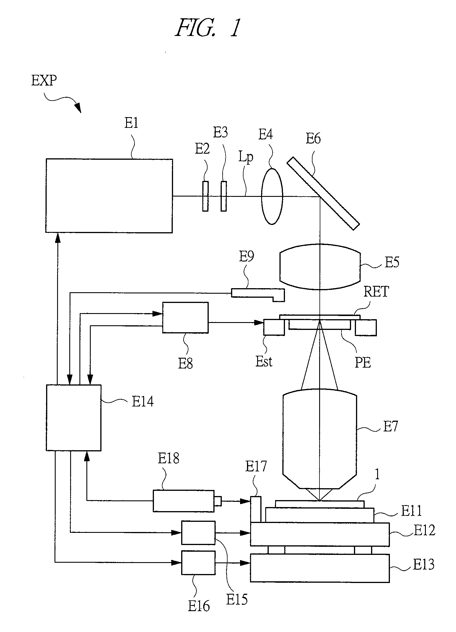
[0058]FIG. 1 is a diagram showing an example of the configuration of an exposure device. In FIG. 1, only the parts needed to describe the functions of the exposure device is shown, and the other parts needed for ordinary exposure devices (a scanner and a stepper) are the same in the ordinary range.

[0059]An exposure device EXP is a scanning type reduced projection exposure device (scanner) with a reduction ratio of 4:1, for example. An exposing condition of the exposure device EXP is as follows, for example. That is, a KrF excimer laser light with an exposure wavelength of about 248 nm is used for an exposure light Lp, the numerical aperture of an optical lens is NA=0.65, the shape of illumination is circular, and the coherency (σ: sigma) value=0.7. However, the exposure light Lp is not limited to the above-mentioned value, and modifications are possible; for example, the g ray, the i ray, the ArF excimer laser light (wavelength of 193 nm), or the F2 (fluorine) gas laser light (wavel...

embodiment 2

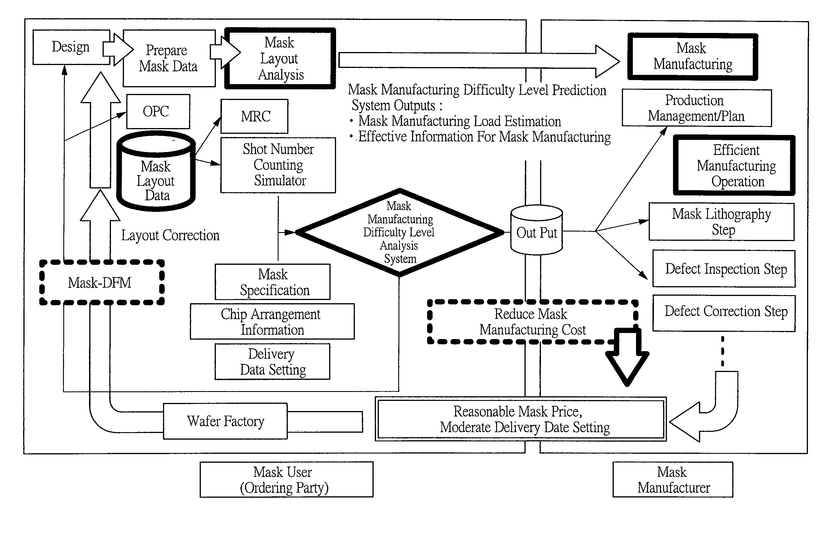
[0082]Design intent in the present embodiment means a priority classification of layout according to a designer's intention, and this information can be incorporated in mask layout data to be used for mask manufacturing. For example, the information is used for operation of the mask defect standard set depending on the priority of patterns, including: (a) different inspection sensitivity according to the priority; (b) differentiation of the determination of a defect after detection; and (c) differentiation of correction of a detected defect and an inspecting method and standard after correction. The design intent can be used to ease the defect standard of a portion with a relatively low priority of a pattern, and relatively reduce the load of the defect inspection and the defect correction. In addition, since the load on mask manufacturing differs according to the priority of a pattern, the load of the actual defect guarantee step of the whole chip (or mask) can be predicted by calc...

embodiment 3

[0084]Among the defect guarantee load index DAT described in Embodiment 1, a defect correction step set up time is related to a defect correction load, and the defect correction step set up time is related to the number of the defects to be corrected. The number of defects is related to the aperture area (area of a mask pattern drawing part). FIG. 8 shows the relation of the number of defects and the aperture ratio for each mask of the masks for products with a minimum feature size of about 90 nm on a chip. The number of defects is influenced by the quality of a material used for mask manufacturing, a situation of the manufacturing step, a condition of the manufacturing step, etc. and, as shown in FIG. 8, the number of generated defects increases with the increase of the aperture ratio. That is, the probability of defects being generated is larger when the area of the pattern to be guaranteed is larger, resulting in heavier load of defect correction. Especially, in the defect guaran...


PUM


Abstract

A technique for quantitatively expressing a manufacturing difficulty level of a photomask and for efficiently manufacturing the photomask is provided. A mask manufacturing difficulty level different for each mask layout, product, and mask layer is relatively recognized with a mask manufacturing load index calculated by a mask manufacturing load prediction system, and when layout correction is possible, the final layout is corrected to a layout with a low difficulty level, and a mask ordering party provides a mask manufacturer with information regarding the mask manufacturing difficulty level in an early stage. The mask manufacturing load index is expressed with a defect guarantee load index and a lithography load index.

Description

CROSS-REFERENCE TO RELATED APPLICATION[0001]The present application claims priorities from Japanese Patent Application No. JP 2007-239303 filed on Sep. 14, 2007, and Japanese Patent Application No. JP 2008-175491 filed on Jul. 4, 2008, the contents of which are hereby incorporated by reference into this application.TECHNICAL FIELD OF THE INVENTION[0002]The present invention relates to a manufacturing technique of a photomask. More particularly, the present invention relates to a technique effective for improving efficiency of manufacturing masks.BACKGROUND OF THE INVENTION[0003]In recent years, an effort has been undertaken to improve a resolution performance on semiconductor wafers (hereinafter, simply referred to as wafer) so as to develop more advanced semiconductor devices with a continuous attempt for a finer design (circuit pattern) size and RET (Resolution Enhancement Technique). Therefore, photomasks also have introduced finer design rules, higher integration, more complex O...

Claims


Application Information

Patent Timeline
IPC IPC(8): G06F17/50
CPCG03F1/14G03F1/00
Inventor NAGAMURA, YOSHIKAZUNARUKAWA, SHOGO
Owner DAI NIPPON PRINTING CO LTD
Why Eureka
Try Eureka