
Laser Device Using an Inorganic Electro-Luminescent Material Doped With a Rare-Earth Element

a rare earth element and laser device technology, applied in semiconductor lasers, laser details, excitation process/apparatus, etc., can solve the problems of high packaging cost, light source problems, and serious drawbacks of porous silicon in reproducibility and reliability of luminescent devices,

Inactive Publication Date: 2009-03-26
KYUNGPOOK NAT UNIV IND ACADEMIC COOP FOUND
View PDF2 Cites 19 Cited by
  • Summary
  • Abstract
  • Description
  • Claims
  • Application Information

AI Technical Summary

Benefits of technology

[0013]The invention has been made to solve the foregoing problems of the prior art and therefore an object of the invention is to provide a laser device using an inorganic EL material doped with a rare-earth element that can be fabricated on a silicon substrate (or glass substrate) using an inorganic EL material and that can provide a long-wavelength light source in which electric pumping is possible.

Problems solved by technology

In manufacturing various optical elements to be used in the silicon photonics, the light source may be problematic.
The porous silicon has a serious drawback in reproducibility and reliability of a luminescent device because of high reactivity in a sponge structure.
Since this method should externally integrate a special LD chip, the packaging cost also increases.
This is disadvantageous in manufacturing an optical communication device in comparison with a method of bonding III-V light source chips to a silicon semiconductor.
Even though the attachment of devices having heterogeneous materials is not problematic with the development of a device packaging method, it is still avoided due to the increased cost and poor scalibility.
For this reason, the existing methods are difficult to take full advantage of a mass production technology developed for a silicon semiconductor device, thereby resulting in an increase in cost.

Method used


Image

  • Laser Device Using an Inorganic Electro-Luminescent Material Doped With a Rare-Earth Element
  • Laser Device Using an Inorganic Electro-Luminescent Material Doped With a Rare-Earth Element
  • Laser Device Using an Inorganic Electro-Luminescent Material Doped With a Rare-Earth Element

Examples


Embodiment Construction

[0021]Exemplary embodiments of the invention now will be described more fully with reference to the accompanying drawings, in which exemplary embodiments of the invention are shown. This invention may, however, be embodied in many different forms and should not be construed as limited to the exemplary embodiments set forth herein. In the drawings, elements that are not directly related to the description of the invention are omitted for convenience of explanation. Like reference numerals refer to like elements throughout this application.

[0022]In addition, unless explicitly described to the contrary, the word “comprise” and variations such as “comprises” or “comprising” will be understood to imply the inclusion of stated elements but not the exclusion of any other elements. In addition, the word “part”, “unit”, “module”, “block”, or the like will be understood to indicate a unit for processing at least one function or operation, which may be realized by hardware, software, or a comb...


PUM


Abstract

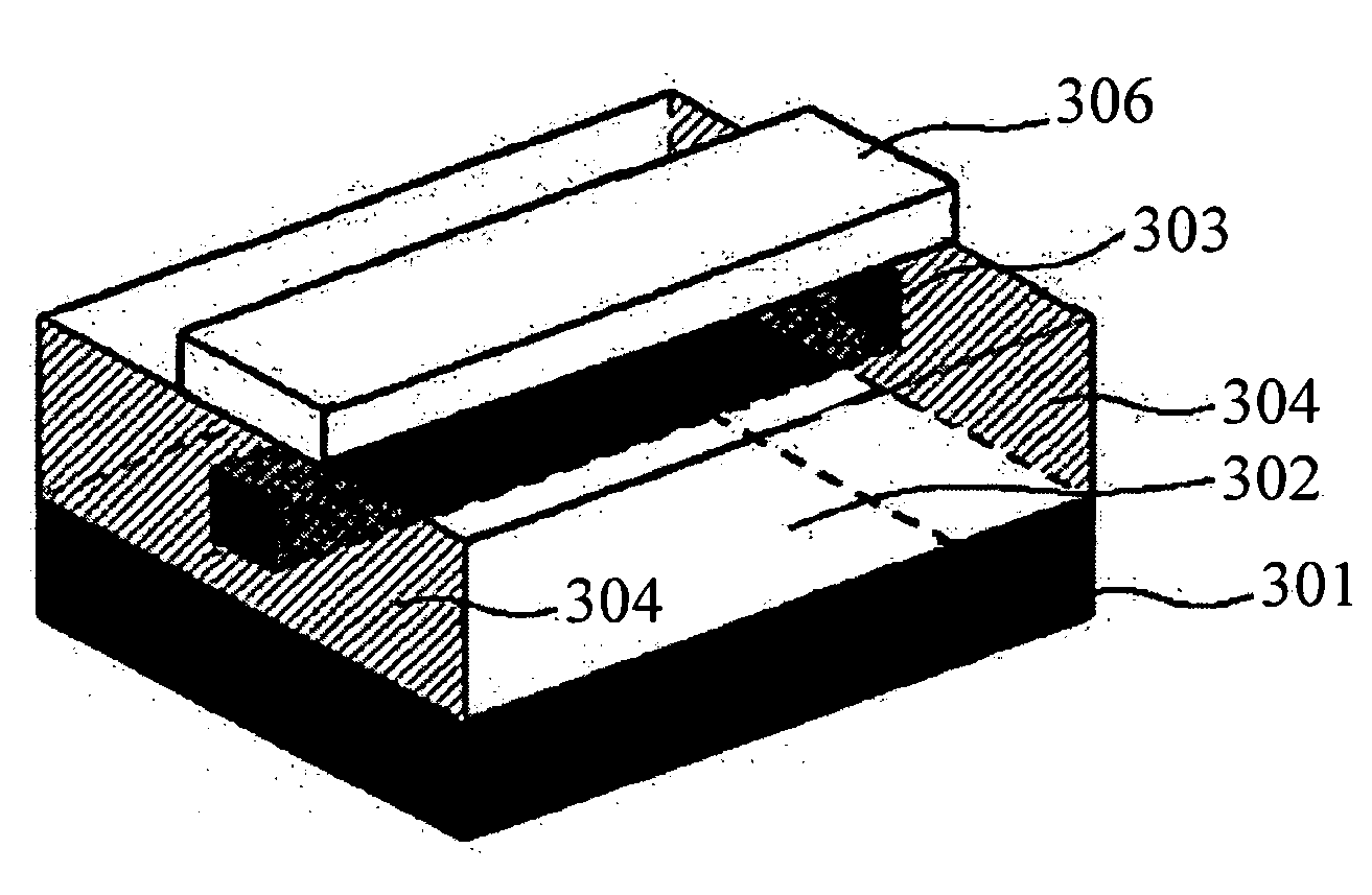
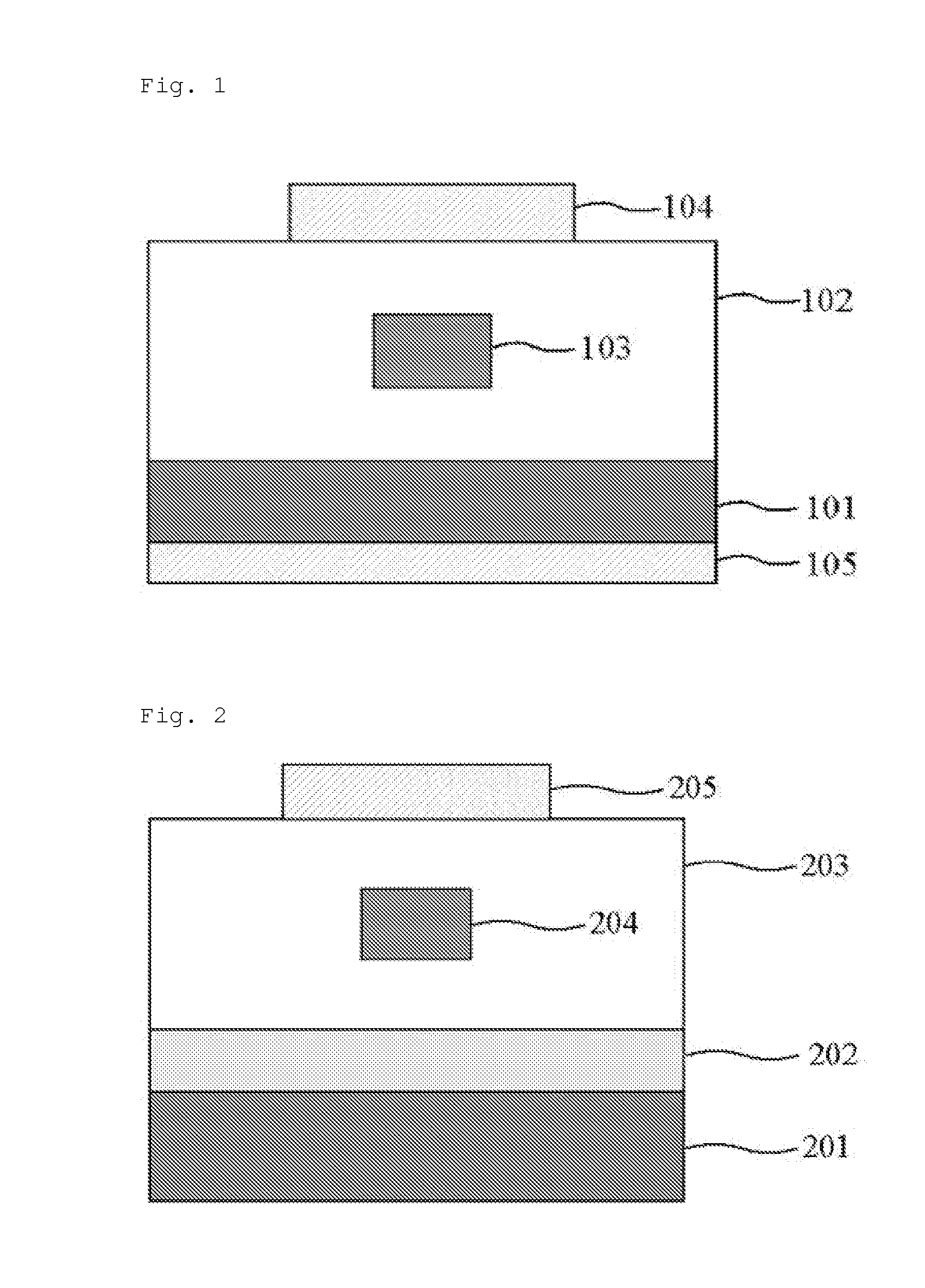
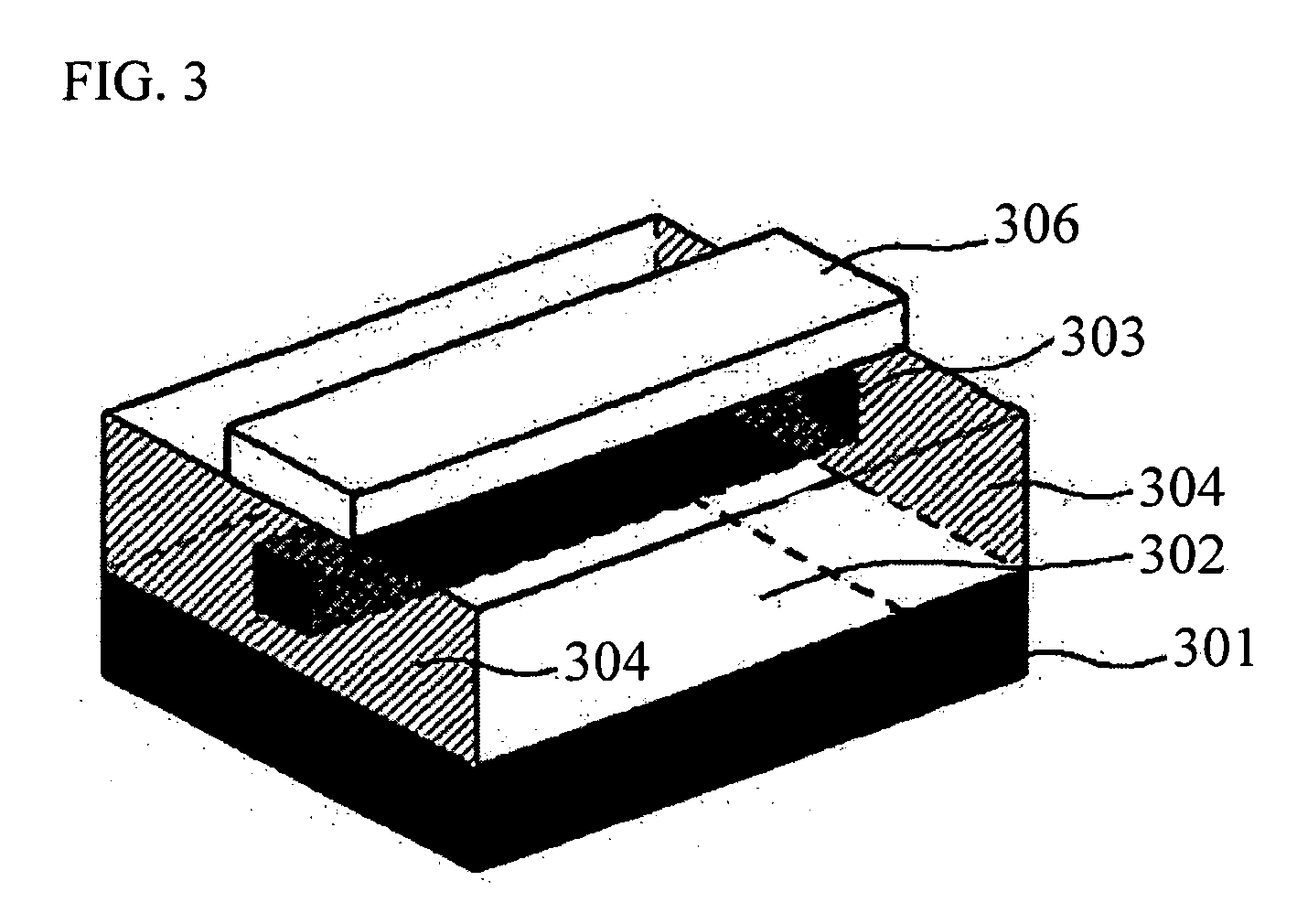
A laser device using an inorganic electro-luminescent material doped with a rare-earth element is provided. A dielectric layer such as SiO2 is arranged on a silicon substrate. A polycrystalline thin film of Er-doped ZnS or ZnSe is arranged on the dielectric layer. An electrode is formed on the dielectric layer. After a waveguide structure is substantially formed, a reflector is formed at both ends of the waveguide structure to form a laser resonator. An active medium is a polycrystalline material of Er-doped ZnS or ZnSe. When an AC voltage is applied between an electrode attached to the substrate and an electrode attached to an uppermost part, the effect of emitting light at 1550 nm and generating population inversion is used.

Description

CLAIM OF PRIORITY[0001]This application makes reference to and claims all benefits accruing under 35 U.S.C. §119 from an application for “LASER DEVICE USING AN INORGANIC ELECTRO-LUMINESCENT MATERIAL DOPED WITH RARE-EARTH METAL,” earlier filed in the Korean Intellectual Property Office on Apr. 23, 2007 and there duly assigned Serial No. 2007-0038205.BACKGROUND OF THE INVENTION[0002]1. Field of the Invention[0003]The present invention relates to a semiconductor laser device, and more particularly to a laser device using an inorganic electro-luminescent (EL) material doped with a rare-earth element.[0004]2. Description of the Related Art[0005]At present, a silicon (Si) semiconductor process technology is precise enough to implement a line width as small as 50 nm, which is the motive of improving the degree of integration and speed. A highly integrated chip may be produced at low cost on the basis of a large-sized wafer processing technology. Recently, an attempt is being made to manufa...

Claims


Application Information

Patent Timeline
IPC IPC(8): H01S5/00
CPCH01S3/063H01S3/0635H01S3/09H01S3/178H01S3/1628H01S3/1655H01S3/1685H01S3/1608H01S5/00
Inventor JU, YOUNG-GU
Owner KYUNGPOOK NAT UNIV IND ACADEMIC COOP FOUND
Learn More