

Printed circuit board design support method and apparatus
a printed circuit board and support method technology, applied in the direction of cad circuit design, program control, instruments, etc., can solve the problems of increasing the possibility of error and oversight during the determination, unnecessary electromagnetic wave (radiation noise) emissions, and determining the position of the vias takes considerable time, so as to simplify the determination of an area
- Summary
- Abstract
- Description
- Claims
- Application Information
AI Technical Summary
Benefits of technology
Problems solved by technology
Method used
Image

Examples
first exemplary embodiment
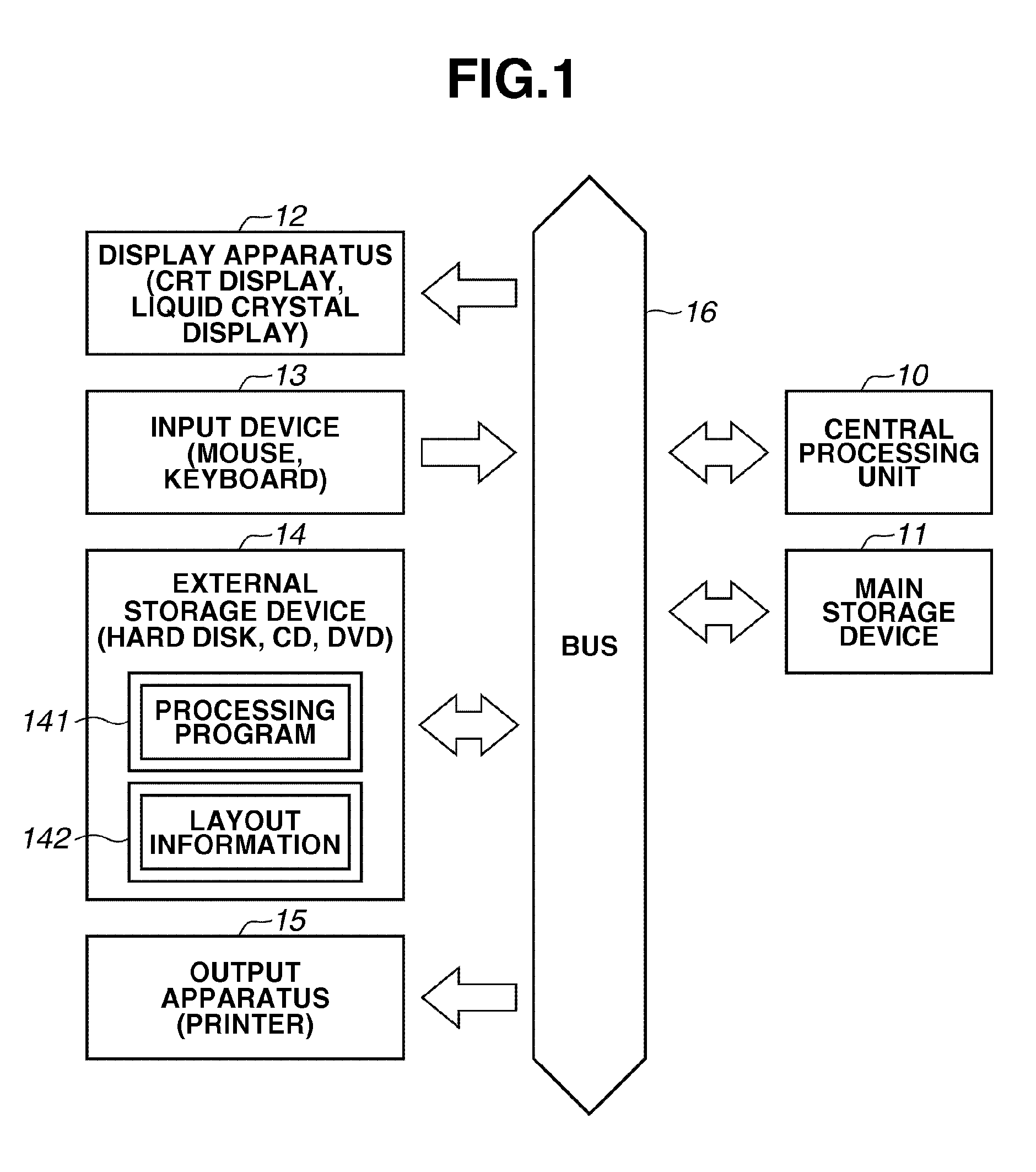
[0033]FIG. 1 illustrates a configuration of a printed circuit board design support apparatus according to a first exemplary embodiment of the present invention. The printed circuit board design support apparatus includes a central processing unit (CPU) 10, a main storage device 11, a display apparatus 12, an input device 13, an external storage device 14, an output apparatus (printer) 15, and a bus 16.
[0034]The CPU 10 controls the entire printed circuit board design support apparatus. The main storage device 11 is a read-only storage device (read-only memory (ROM)) and / or a storage device (random access memory (RAM)), which the CPU 10 reads / writes during calculation processing. The display apparatus 12 is, for example, a cathode-ray tube display or a liquid crystal display. The input device 13 is, for example, a mouse and / or a keyboard. The external storage device 14 is used for reading data from and / or writing data to a recording medium such as a hard disk, a flexible disk, a compa...
second exemplary embodiment
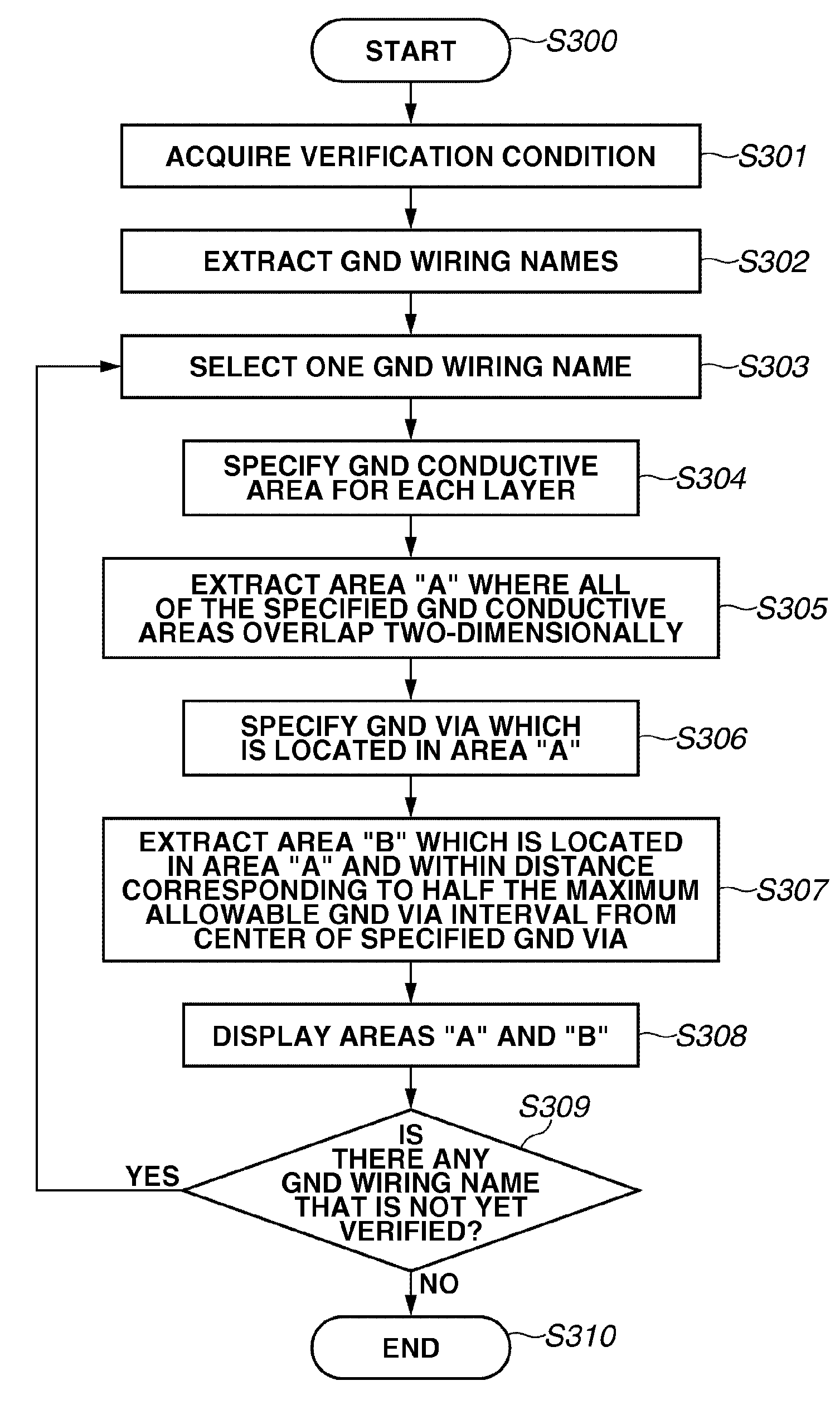
[0083]A second exemplary embodiment of the present invention will be described. According to the first exemplary embodiment, all of the GND conductive areas of the extracted GND wirings are verified. According to the second exemplary embodiment, the GND conductive areas to be verified can be selected by the user. Although some parts of a processing program 141 of the second exemplary embodiment differs from the first exemplary embodiment, the rest is similar to the first exemplary embodiment. FIG. 11 is a flowchart illustrating an operation of a printed circuit board design support apparatus according to the second exemplary embodiment. Mainly, processes which differ from those illustrated in FIG. 10 are described.
[0084]First, the graphic calculation unit 22 performs the processes in steps S300 to S302 as in the first exemplary embodiment.
[0085]In step S1000, the graphic calculation unit 22 checks the layout information 142 and determines whether a GND wiring name which is not yet s...
third exemplary embodiment
[0103]A third exemplary embodiment of the present invention will be described. According to the third exemplary embodiment, a design considering high-speed interconnection as well as the GND wirings becomes possible. Although some of a processing program 141 of the third exemplary embodiment differs from the first exemplary embodiment, the rest is similar to the first exemplary embodiment. FIG. 16 is a flowchart illustrating an operation of a printed circuit board design support apparatus according to the third exemplary embodiment. Mainly, processes which differ from those illustrated in FIG. 10 are described.
[0104]After the process is started in step S300, the display unit 23 displays an entry screen for prompting a user to enter a verification condition. In step S301, the graphic calculation unit 22 acquires the verification condition input through the input unit 20. As the verification condition, a maximum allowable high-speed interconnection via-GND via interval L2 as well as t...
PUM
 Abstract
Description
Claims
Application Information