Assembly comprising an electromagnetically screened SMD component, method and use

a technology of electromagnetic screening and component, applied in the direction of electrical equipment, climate sustainability, printed circuit aspects, etc., can solve the problem that the related art may not provide blind holes, and achieve the effect of maximizing the screening effect of the electromagnetic screen

Active Publication Date: 2009-04-02
OTICON
View PDF14 Cites 40 Cited by
  • Summary
  • Abstract
  • Description
  • Claims
  • Application Information

AI Technical Summary

Benefits of technology

[0012]An object of the present disclosure is to provide an electronic component assembly that is suitable for integration on a substrate in a mixed analogue digital environment. It is an object of the disclosure to provide a component assembly that can shield a predefined group of SMD components against electromagnetic radiation at radio frequencies (RF). It is an object of the disclosure to provide a component assembly that can shield a predefined group of SMD components against static and relatively low frequency electric fields. It is an object of the disclosure to provide a component assembly that can shield a predefined group of SMD components against static and relatively high frequency electric fields.
[0020]An advantage of the disclosure is that a predefined arrangement of SMD components, e.g. a single SMD component or a group of SMD components, can be independently shielded to allow for an increased density of components on a substrate. Critical input components, such as RF-receiver and sensitive analogue circuits in general, that are located near a source of electromagnetic radiation (e.g. clock generator and digital circuits in general) can be advantageously arranged in a component assembly according to the disclosure, whereas uncritical components or components located farther away from the source of electromagnetic radiation can be left unshielded, having the advantage that no post-shielding-process is needed after the (shielded) component assembly or assemblies and (un-shielded) components have been mounted on their common substrate, e.g. a PCB. Also groups of components, which are sources of electromagnetic radiation, and therefore can disturb other circuits, can be individually arranged as electronic component assemblies according to the disclosure, and thereby have their electromagnetic radiation reduced. This has the advantage of allowing them to be located relatively closer to other circuits on a substrate than would otherwise be practically possible (while the total arrangement of components and circuits are still being functional).
[0030]In an embodiment, the at least one SMD component has a substrate-facing surface that is adapted for facing a substrate for electrical connection of a terminal of the component to the substrate. In an embodiment, the electrically insulating layer and the electromagnetic screen cover at least a part of some of the surfaces of the SMD component, such as all but the substrate-facing surface. Optionally, the electrically insulating layer and the electromagnetic screen cover (at least) a major part of the area of all but the substrate-facing surface. This has the advantage of maximizing the screening effect of the electromagnetic screen for components of the assembly in directions away from the substrate on which the component assembly is intended for being mounted. In an embodiment, the electrically insulating layer and optionally also the electromagnetic screen cover a part of the substrate-facing surface (e.g. such parts which does not contain electrical terminals).

Problems solved by technology

Since the metallic film is formed on the side surfaces of the sealing resin and the side surfaces of the multi-layered substrate, when the metallic film is formed by a plating method, the blind hole may not be provided in the related art.

Method used


Image

  • Assembly comprising an electromagnetically screened SMD component, method and use
  • Assembly comprising an electromagnetically screened SMD component, method and use
  • Assembly comprising an electromagnetically screened SMD component, method and use

Examples


Embodiment Construction

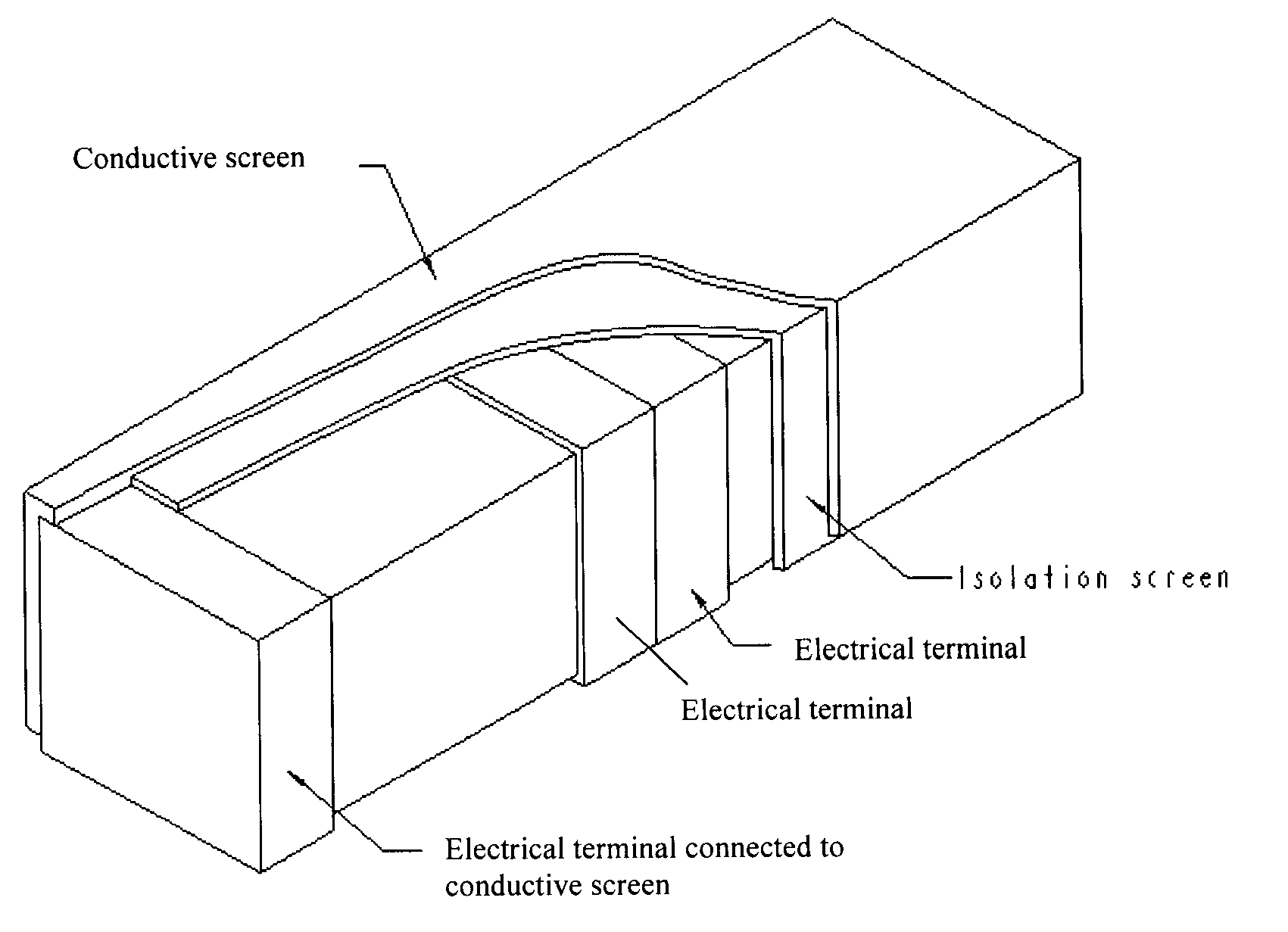
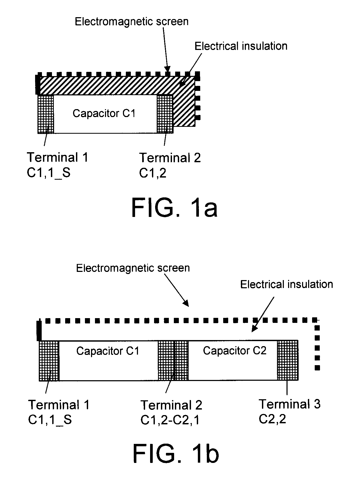
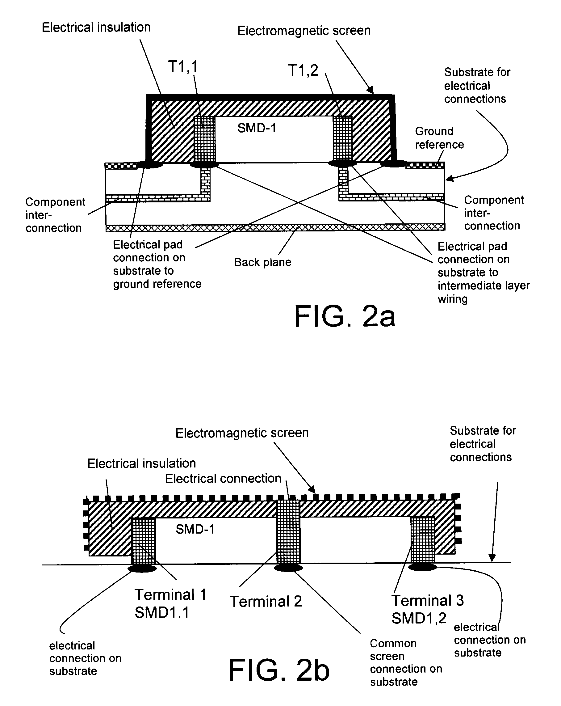
[0094]In order to screen SMD components from undesired electromagnetic fields (from neighbouring devices on a common substrate or from a neighbouring substrate in the same device or from another separate device) a screen is put around the surface, preferably on all sides except one. The non-shielded side is preferably the solder side.

[0095]The shield may be connected in various ways.

[0096]1. Connected to an extra dedicated shield terminal.

[0097]2. Connected to an electrical terminal (e.g. at one end) of a component in the assembly.

[0098]When the device, which the assembly is part of, e.g. a hearing instrument, includes computer technology (e.g. a digital signal processor) and wireless technology (e.g. a BlueTooth or FM receiver and / or transmitter, etc.) at the same time, the use of component assemblies according to the disclosure will facilitate the use of a more sensitive wireless receiver and / or a lower signal level in the transmitter.

[0099]Also with respect to analogue signals, t...


PUM

PropertyMeasurementUnit
frequenciesaaaaaaaaaa

Abstract

The disclosure relates to an electronic component assembly including at least one SMD component (11) having a number of external surfaces (111) limited by edges (112) and at least two electrical terminals (113), an electromagnetic screen (12) for limiting the electromagnetic coupling to and from the SMD component or components, and an electrically insulating layer (13) located between at least one of the surfaces and the electromagnetic screen. The disclosure furthermore relates to a method of manufacturing an electronic component assembly and to the use of an electronic component assembly.

Description

TECHNICAL FIELD[0001]The present disclosure relates to surface mount components in instruments (e.g. hearing instruments), where e.g. analogue, digital and wireless technology must coexist in very densely packed units.[0002]The disclosure relates specifically to an electronic component assembly comprising at least one surface mount component (SMC) and an electromagnetic screen for limiting the electromagnetic coupling to and from the surface mount component(s) and an electrically insulating layer located between at least one surface of the surface mount component(s) and the electromagnetic screen. The disclosure further relates to an intermediate product comprising an electronic component assembly.[0003]The disclosure furthermore relates to a method of manufacturing an electronic component assembly, to a method of selectively protecting one or more electronic SMD components from electromagnetic coupling to one or more other electronic components without an electromagnetic screen and...

Claims


Application Information

Patent Timeline
Patent Type & Authority Applications(United States)
IPC IPC(8): H05K1/02H05K3/00
CPCH05K1/0218Y10T29/49124H05K2201/10636H05K1/181H05K9/0022Y02P70/50
Inventor NIELSEN, CHRISTIAN
Owner OTICON
Why Eureka
Try Eureka