Semiconductor light emitting device and method of manufacturing the same

a technology of semiconductors and light emitting devices, which is applied in the manufacture of semiconductor/solid-state devices, semiconductor devices, and semiconductor devices. it can solve the problems of unfavorable increase of forward voltages higher than the desired level, and achieve the effect of improving the characteristic of the nitrogen fa

Inactive Publication Date: 2009-04-02
SAMSUNG ELECTRONICS CO LTD
View PDF4 Cites 22 Cited by
  • Summary
  • Abstract
  • Description
  • Claims
  • Application Information

AI Technical Summary

Benefits of technology

[0021]A laser treatment may be performed on the nitrogen face of the GaN substrate before t

Problems solved by technology

However, a semiconductor light emitting device including the n-type electrode using general n-type electrode materials such as Ti, Cr,

Method used


Image

  • Semiconductor light emitting device and method of manufacturing the same
  • Semiconductor light emitting device and method of manufacturing the same
  • Semiconductor light emitting device and method of manufacturing the same

Examples


Embodiment Construction

[0029]Exemplary embodiments of the present invention will be described below in more detail with reference to the accompanying drawings. The present invention may, however, be embodied in different forms and should not be constructed as limited to the embodiments set forth herein. Rather, these embodiments are provided so that this disclosure will be thorough and complete, and will fully convey the scope of the present invention to those skilled in the art.

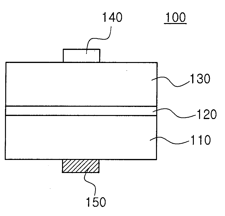
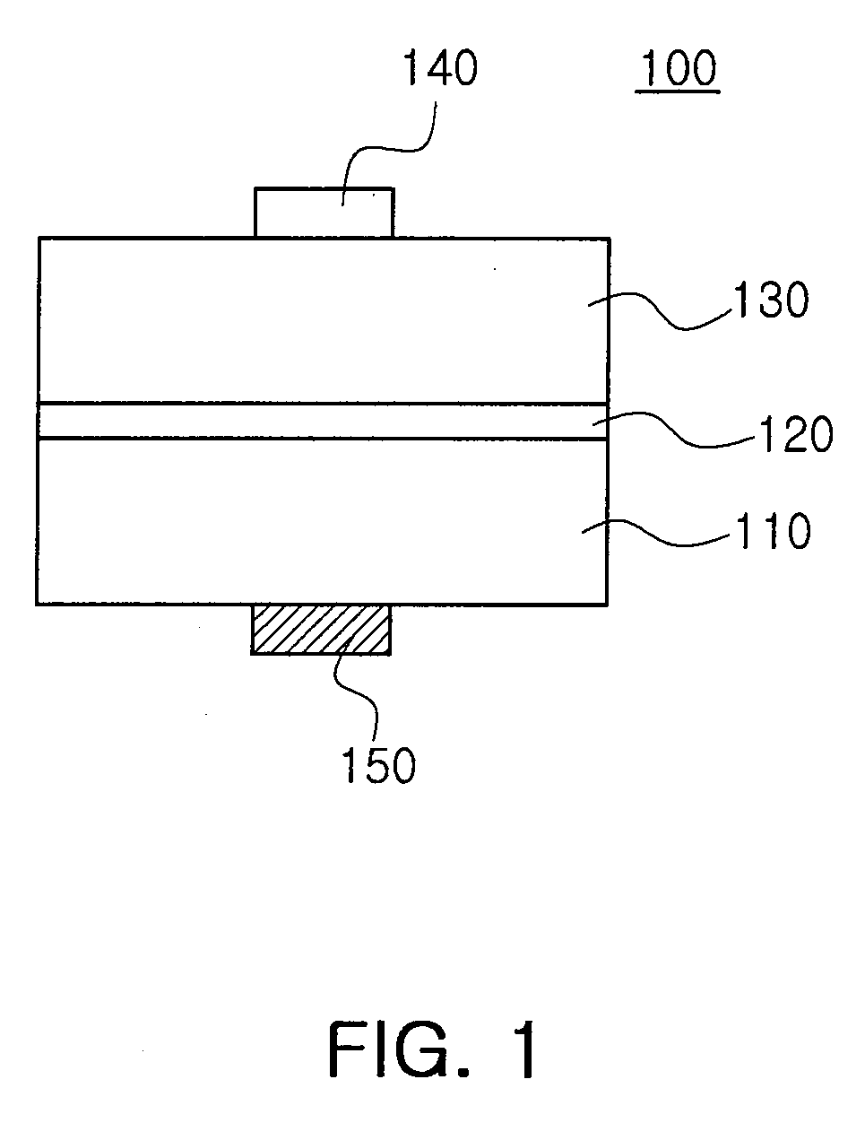
[0030]FIG. 1 is a cross-sectional view of a semiconductor light emitting device 100 according to an embodiment of the present invention. Referring to FIG. 1, the semiconductor light emitting device 100 includes an n-type GaN semiconductor layer 110, an active layer 120 formed on a gallium face of the n-type GaN semiconductor layer 110, a p-type semiconductor layer 130 formed on the active layer 120, and an n-type electrode 150 formed on a nitrogen face of the n-type GaN semiconductor layer 110 and including a lanthanum (La)-nickel...


PUM


Abstract

Disclosed are a semiconductor light emitting device, which can improve characteristics of the semiconductor light emitting device such as a forward voltage characteristic and a turn-on voltage characteristic, increase light emission efficiency by lowering an input voltage, and increase reliability of the semiconductor light emitting device by a low-voltage operation, and a method of manufacturing the same. The semiconductor light emitting device includes: an n-type GaN semiconductor layer; an active layer formed on a gallium face of the n-type GaN semiconductor layer; a p-type semiconductor layer formed on the active layer; and an n-type electrode formed on a nitrogen face of the n-type GaN semiconductor layer and including a lanthanum (La)-nickel (Ni) alloy.

Description

CROSS-REFERENCE TO RELATED APPLICATIONS[0001]This application claims the priority of Korean Patent Application No. 10-2007-0098105 filed on Sep. 28, 2007, in the Korean Intellectual Property Office, the disclosure of which is incorporated herein by reference.BACKGROUND OF THE INVENTION[0002]1. Field of the Invention[0003]The present invention relates to a semiconductor light emitting device and a method of manufacturing the same, and more particularly, to a semiconductor light emitting device which can improve characteristics of the semiconductor light emitting device such as a forward voltage characteristic and a turn-on voltage characteristic, increase light emission efficiency by lowering an input voltage, and increase reliability of the semiconductor light emitting device by a low-voltage operation, and a method of manufacturing the same.[0004]2. Description of the Related Art[0005]In general, a semiconductor light emitting device is a device in which a semiconductor material em...

Claims


Application Information

Patent Timeline
IPC IPC(8): H01L33/00H01L33/06H01L33/40H01L33/32
CPCH01L33/40H01L33/32
Inventor SONG, SANG YEOBLEE, JIN HYUNKIM, YU SEUNGCHOI, KWANG KICHOI, PUN JAEKIM, HYUN SOOLEE, SANG BUM
Owner SAMSUNG ELECTRONICS CO LTD
Why Eureka
Try Eureka