

Information recording medium and method for manufacturing same
- Summary
- Abstract
- Description
- Claims
- Application Information
AI Technical Summary
Benefits of technology
Problems solved by technology
Method used
Image

Examples
embodiment 1
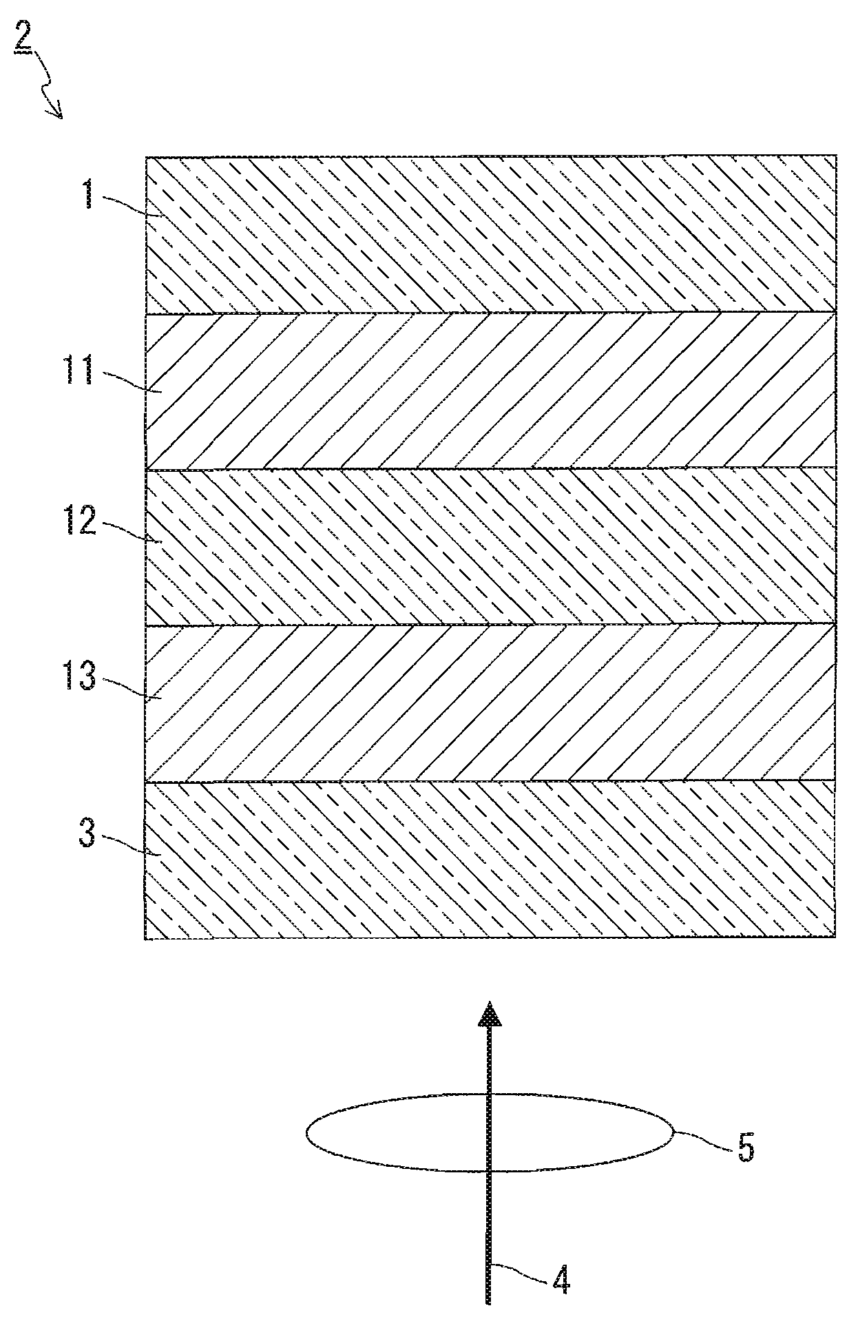
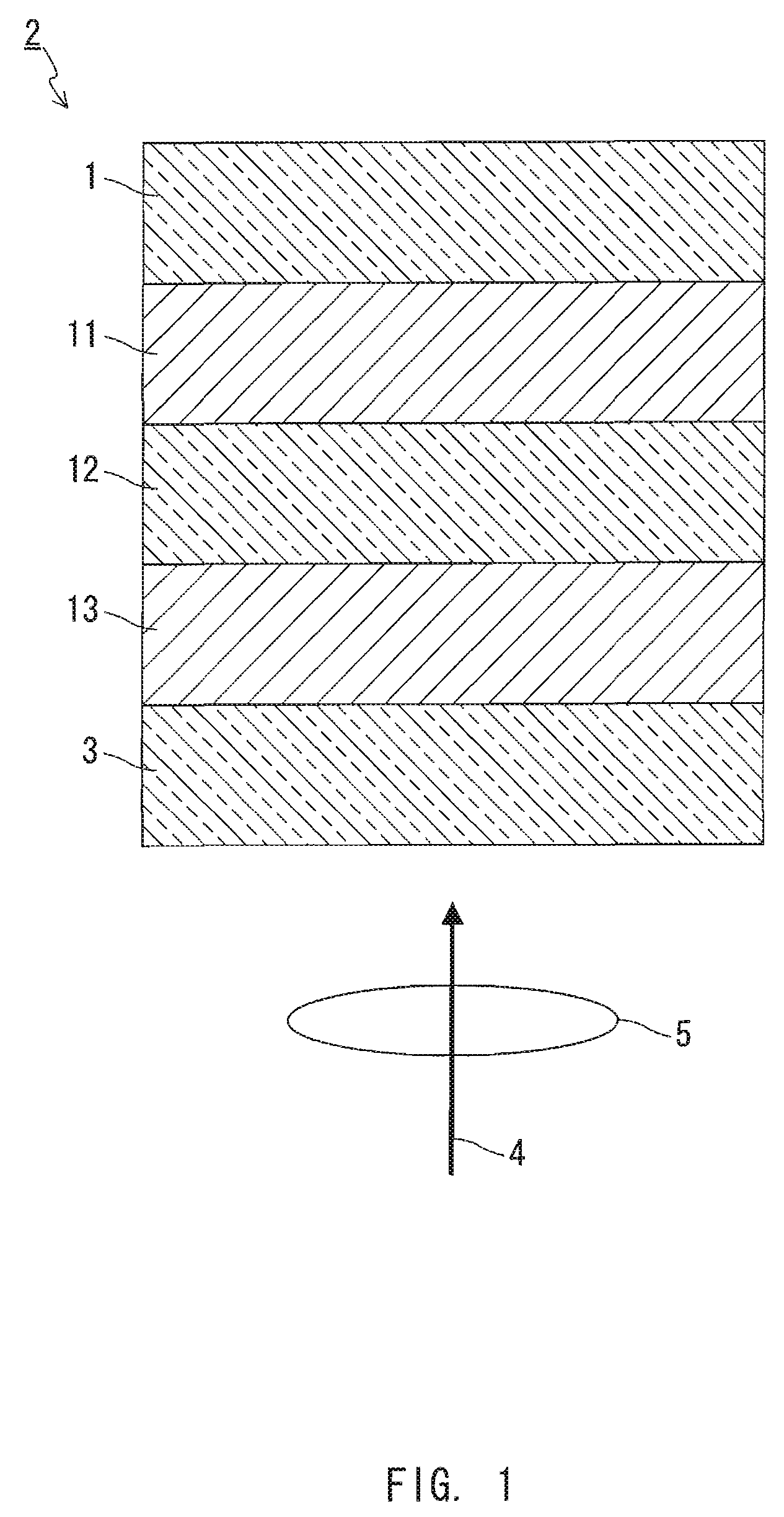
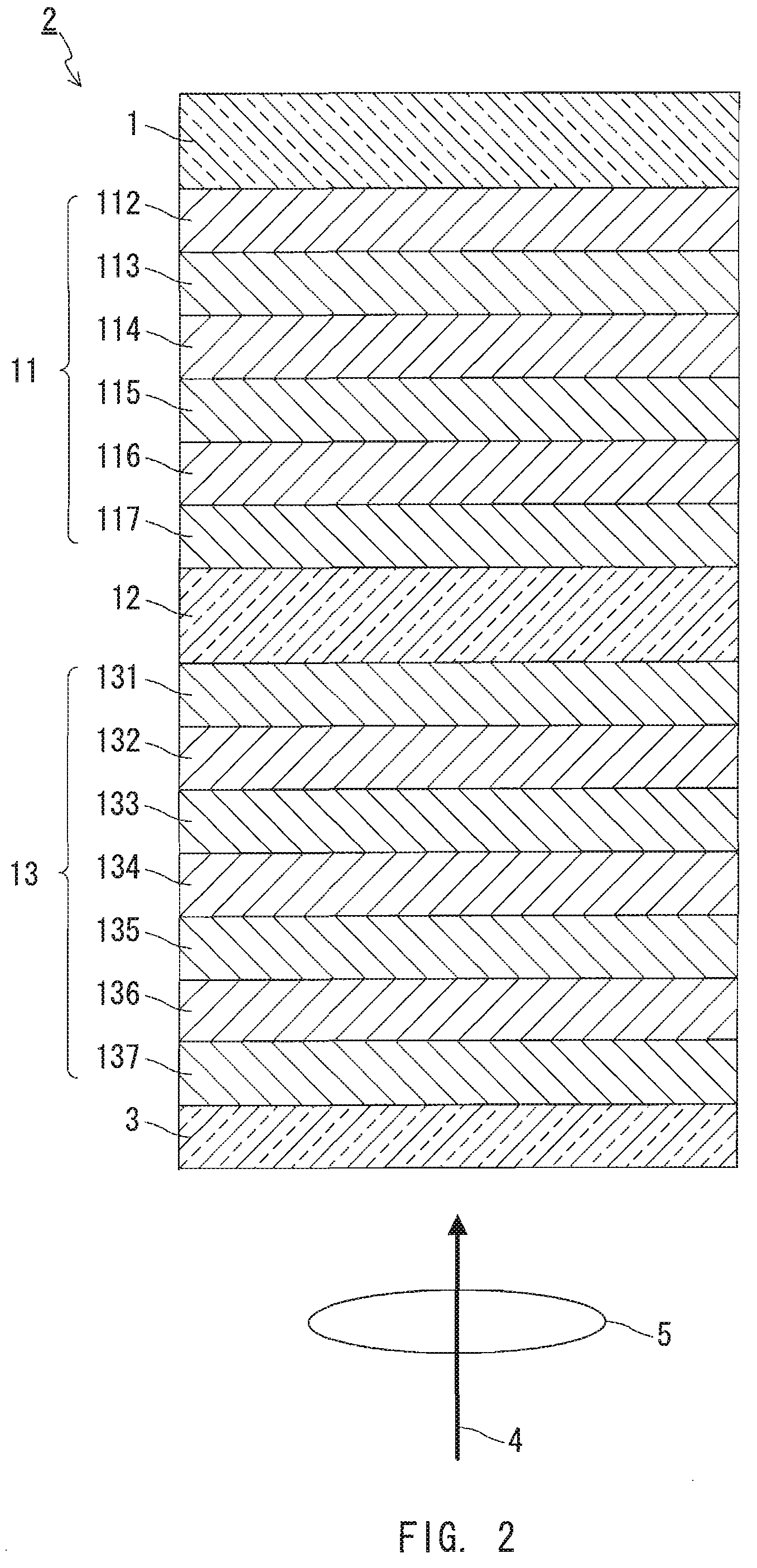
[0032]In Embodiment 1, an example of an information recording medium of the present invention is described. FIG. 1 shows a partial sectional view of an information recording medium of Embodiment 1. The information recording medium 2 of this embodiment is an optical information recording medium that can record and reproduce information through irradiation with a laser beam 4 focused through an objective lens 5.
[0033]The information recording medium 2 includes a first information layer 11, a separation layer 12, a second information layer 13, and a transparent layer 3 on a substrate 1 in this order. That is, the information recording medium 2 of this embodiment is an example obtained when N=2 and L=2 in the information recording medium of the present invention, and the second information layer 13 corresponds to the N-th information layer and the L-th information layer. Furthermore, in the information recording medium 2 of this embodiment, the transparent layer 3 side is the laser beam...
embodiment 2
[0099]In Embodiment 2, another example of an information recording medium of the present invention is described. FIG. 5 shows a partial sectional view of the information recording medium according to Embodiment 2. The information recording medium 8 of this embodiment is an optical information recording medium that can record and reproduce information through irradiation with a laser beam 4 focused through an objective lens 5 as in the case of the information recording medium 2 described in Embodiment 1.
[0100]The information recording medium 8 has a structure in which a second information layer 13 and a first information layer 11 are stacked on a first substrate 53 and a second substrate 51, respectively, and the first information layer 11 and the second information layer 13 are bonded to each other with an adhesive layer 52 being interposed therebetween. That is, the information recording medium 8 of this embodiment is an example obtained when N=2 and L=2 in the information recordin...
embodiment 3
[0127]In Embodiment 3, another example of an information recording medium of the present invention is described. FIG. 9 shows a partial sectional view of the information recording medium according to Embodiment 3. The information recording medium 15 of this embodiment is an optical information recording medium that can record and reproduce information through irradiation with a laser beam 4 focused through an objective lens 5 as in the case of the information recording medium 2 described in Embodiment 1.
[0128]The information recording medium 15 is formed by stacking a second information layer 13, a separation layer 12, and a first information layer 11 on a substrate 55 and bonding the first information layer 11 and a dummy substrate 60 together, with an adhesive layer 52 being interposed therebetween. That is, the information recording medium 15 of this embodiment has a structure obtained when N=2 and L=2 in the information recording medium of the present invention, and the second i...
PUM
 Abstract
Description
Claims
Application Information